


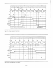
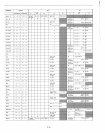

NOTES:
1.
The
first
memory
cycle
(M
1)
is
always an
instruction
fetch;
the
first (or only)
byte,
containing
the
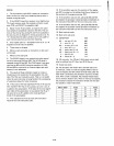
op
code,
is
fetched during
this
cycle.
2.
If
the
READY
input
from
memory
is
not
high during
T2
of
each memory cycle,
the
processor will
enter
a wait
state (TW)
until READY
is
sampled as high.
3.
States
T4
and
T5
are present, as required,
for
opera·
tions
which
are
completely
internal
to
the
CPU.
The
con-
tents
of
the
internal bus during
T4
and
T5
are available
at
the
data
bus;
this
is
designed for testing purposes
only.
An
"X"
denotes
that
the
state
is
present,
but
is
only
used for
such internal
operations
as instruction decoding.
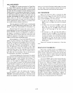
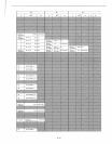
4.
Only
register pairs
rp
= B (registers B and
C)
or
rp=
D
(registers D and
E)
may be specified.
5. These states are skipped.
6. Memory read sub-cycles; an
instruction
or
data
word
will be read.
7. Memory write sub-cycle.
8.
The
READY signal
is
not
required during
the
second
and
third
sub·cycles (M2 and M3).
The
HOLD signal is
accepted during
M2
and
M3.
The
SYNC signal
is
not
gene-
rated during
M2
and M3. During
the
execution
of
DAD,
M2
and M3 are required for an internal register-pair
add;
memory
is
not
referenced.
9.
The
results
of
these
arithmetic,
logical
or
rotate
in-
structions
are
not
moved into
the
accumulator
(A) until
state
T2
of
the
next
instruction
cycle.
That
is,
A
is
loaded
while
the
next
instruction
is
being
fetched;
this
overlapping
of
operations
allows for faster processing.
10.
If
the
value
of
the
least significant 4-bits
of
the
accumu-
lator
is
greater
than
9
~
if
the
auxiliary carry bit
is
set, 6
is
added
to
the
accumulator.
If
the
value
of
the
most
signifi-
cant
4-bits
of
the
accumulator
is
now
greater
than
9,
~
if
the
carry
bit
is
set, 6
is
added
to
the
most significant
4-bits
of
the
accumulator.
11. This represents
the
first sub-cycle (the
instruction
fetch)
of
the
next
instruction cycle.
12.
If
the
condition
was
met,
the
contents
of
the
register
pair
WZ
are
output
on
the
address lines (A()'15) instead
of
the
contents
of
the
program
counter
(PC).
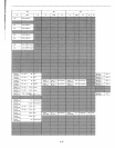
13.
If
the
condition
was
not
met,
sub-cycles M4 and M5
are skipped;
the
processor instead
proceeds
immediately
to
the
instruction
fetch
(Ml)
of
the
next
instruction cycle.
14.
If
the
condition
was
not
met, sub-cycles
M2
and
M3
are skipped;
the
processor instead proceeds immediately
to
the
instruction
fetch
(Ml)
of
the
next
instruction cycle.
15.
Stack
read sub-cycle.
16.
Stack
write sub-cycle.
17.
CONDITION
CCC
NZ
not
zero (Z = 0)
000
Z
zero (Z = 1)
001
NC
no carry (CY = 0)
010
C
carry (CY = 1)
011
PO
parity
odd
(P = 0)
100
PE
parity even
(P
= 1)
101
P
plus (S = 0)
110
M
minus
(S =
1)
111
18.
I/O sub-cycle:
the
I/O
port's
8-bit select
code
is
dupli-
cated
on
address lines 0-7 (A()'7)
and
8-15 (A8-15).
19.
Output
sub-cycle.
20.
The
processor will remain idle in
the
halt
state
until
an
interrupt,
a reset
or
a hold
is
accepted.
When a hold re-
quest
is
accepted,
the
CPU enters
the
hold mode;
after
the
hold mode
is
terminated,
the
processor
returns
to
the
halt
state. After a reset
is
accepted,
the
processor begins execu·
tion
at
memory
location zero.
After
an
interrupt
is
accepted,
the
processor
executes
the
instruction
forced
onto
the
data
bus (usually a
restart
instruction).
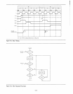
SSS
or
DDD Value
rp
Value
A 111
B
00
B
000
D
01
C
001
H
10
D
010
SP
11
E
011
H
100
L
101
4-20
II
II
IIII
I
I
I'