


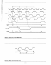
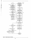
Taking note of asterisked margins shown
on
the comparison
sheet: tAD, tRD, tRR and
tDW,
it is seen that they are all
taken care of by introducing a wait state. The double aster-
isked margins deal with the tRV spec on the 8255A-5,
8253-5 and 8279-5 peripherals. tRV is the time from the rising
edge of WR or
RD
to the next falling edge.
To
allow sufficient
time for this spec it is necessary to delay the commands sent
to these three peripherals. Enough dead time must occur to
make up for the entire negative portion of the margin (for
example: 790ns
in
the 8253-5 medium system). Since in the
8085A-2 every machine cycle is at least 200ns long, 4 ma-
chine cycles are sufficient time to allow peripheral control
signal
recovery
(tRV).
One may notice that
all
of the 8085A instructions take at least
4 T-states (providing a minimum of 800ns) giving ample time
to meet this requirement, just by programming one instruc-
tion
in
between every command sent to the peripheral. I/O
mapped I/O, which results
in
using the Input, Output instruc-
tions has this delay time built
in
when moving the data to be
transferred into the accumulator. With memory mapped I/O,
any instruction that accesses memory for data will provide
the time necessary to not violate
tRV
as a second fetch
is performed.
Bus·
Loading Considerations· Oecoupllng
For the cost conscious designer it is always helpful to know
when buffering is needed and when it is not. How much can I
load the 8085A output pins down?
To
answer this it is helpful
to first list the DC requirements of the common types of logic
loading and compare this to the capabilities of the 8085A.
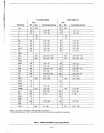
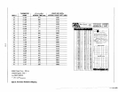
TIL
(single load)
Schottky or
HTIL
MOS
LSTIL
(single load)
Maximum
High-Level
Input
Current
40p,A
40p,A
10p,A
20p,A
Maximum
Low-Level
Input
Current
1.6mA
2.0mA
10p,A
400p,A
The 8085A is capable of
an
10L of 2mA (low) and
10H
of
- 400p,A. With this spec
it
'is
easy
to
come
up
with the pos-
sible combinations of D.C. loading that the designer can use
without bufferi ng:
LOADS
1
TIL
+ 1
LSTIL
1
TIL
+ 36 MOS*
1
SCHOTIKY
or 1
HTIL
40 MOS (various combinations possible)'
5
LSTIL
8085A,
A-2 limiting factor
(level)
LOW
HIGH
LOW
HIGH
LOW
• Exceeds capacitive loading limit,
to
be discussed
If a user exceeds these
DC
loading limitations
he
must buffer
that particular signal. Another factor that the designer must
consider is the capacitive load that is seen by the 8085A
outputs, which may very well
be
excessive even if
DC
loading
is not. One may note that even though the 8085A can handle
a DC load of 40 MOS devices or 36 MOS + 1
TIL,
their
collective input capacitances exceed the 150 pF max spec.
A1-25
The timing specs of the 8085A are guaranteed as long as the
150
pF maximum loading is not exceeded, which includes the
wires, components and parasitics.
If the user exceeds this
value and wants to guarantee his system timing he must
either derate the system timings or use buffering.
What if you choose to ignore this limit and say you can live
with the performance degradation? First the timing perfor-
mance is not all that would degrade, a user must be willing to
give up some reliability of his components (All MOS devices
have this restraint). This is caused
by
the excessive switching
currents that are needed for this extra loading capacitance. If
reliability is not
an
important consideration, the user can load
up to 300 pF
on
the 8085A bus,
but
the following correction
factors must be used to adjust the timings:
for
150
pF < 300 pF add
.13
ns/pF
conversely if less than 150 pF:
for 25 < CL < 150 pF you can subtract .1/ns/pF.
What happens after 300 pF? If the user exceeds this, the
noise levels become excessive and problems will result. How
much
is
to much noise?
350
mvolts zero to peak. Prudent
designers will always buffer when noise approaches this level,
especially
in
the case of going
from
orie board to another.
The above takes into consideration the actual specification
considerations of when to buffer,
but
there are also transmis-
sion line and noise effects that must be considered. When
working with
dynamiC
RAMs small (20-30 ohm) resistors are
commonly put
in
series
in
the address lines to help match
impedance levels and reduce reflections. Note that this re-
sistor should be chosen such that it does not severely degrade
the voltage levels of the signal. Long parallel board traces
with signals that could adversely affect each other should
also
be
avoided to prevent cross talk problems.
By-passing is very important to prevent intermittent problems
which often
plague the board designer. Large bulk capacitors
should be used at strategic locations on the board to prevent
power supply droop. This becomes a major factor when there
are many devices that can turn
on
at once and produce a
considerable drain from the power supply (such as burst re-
fresh
in
dynamic RAM).
To
help smooth out the current spikes that naturally occur
when devices turn
on
and off, it is recommended to liberally
use small capacitors such as the monolithic and other ceramic
capacitors which have low inherent inductance. Attached
in
the
2117
data sheet is a suggested layout of capacitors to
effectively bypass the supply lines to ensure proper system
operation. Cutting corners here
will
often times turn around
and bite you.
Proper layout is
an
important consideration. Power supply
lines should be well gridded to supply sufficient current to all
areas of the board. A strong ground layout is advised to offset
noise problems. Remember if the ground plane moves up in
voltage because
of.
excessive charge dumping
in
a particular
area, the supply will drift up correspondingly. Sensing low
levels often becomes an intermittent problem when proper
ground
is
not provided.