


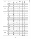
Memory Device Compatibility
Determining What Memory to Select For
Your
Application
When developing a system which will use sufficient memory
to require buffering (see the capacitive
loading section
to
determine when
it
is needed), it is important to understand
how to
select the slowest, lowest cost memory
and
still be
compatible with the bus timings with minimum wait states. A
generalized procedure has been developed in the following
section for determining the memory access needed for dif-
ferent applications and the number of wait states required
(if any).
In
general the amount
oftime
available for access-
ing the memory
can
be
obtained from the following formula:
Available
memory access = 8085A access time (from con-
trol
Signal
of interest) - Buffering/Decoding delay
(to
and
from memory)
The three main
"control" signals of interest which determine
memory access are that of tRD (read to
valid data in), tAD
(valid address
to
valid data in) and tLDR (address latch enable
to valid data in). When dealing with different types of
memories, one or more of these
Signals becomes important.
Even though memory access compatibility
is
probably one of
the most important parameters to consider, as this
is
directly
reflected
in
the price of the memory, it is not the only param-
eter that is important. Some of the other major timing con-
siderations are
as
follows:
WRITE
ENABLE - Is the write enable signal sufficiently long
to
guarantee a write?
Is data set up properly with respect to this write
to
be
compat-
ible
with the memory's requirements?
Is
data held long enough?
DATA
FLOAT - Does your system have sufficient margin to
prevent bus contention?
(Le.,
Does the memory let go of the data bus in time for the
processor to
use
it? Remember that the 8085A shares its
Data Bus with
the
lower 8 addresses.)
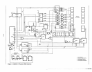
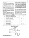
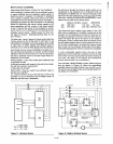
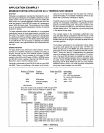
ALE
RD
WR
I
101M
1 I
J
~ ~
8355
OR
A
L
As
-Al0
B755A
'{
~
ADo-AD7
I'r--
r---v'
B085A
...
~
8155
!-
8156
~
I 3.125MHz I 5MHz
tRD
\
300n, \
150n,
tAD
I
575
I 350
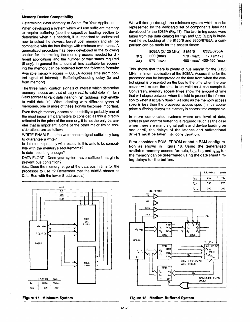
Figure 17. Minimum System
We
will first go through the minimum system which can
be
represented by the dedicated set of components Intel has
developed for the 8085A (Fig.
17).
The two timing specs were
taken from the data
catalog for tRD and tAD (tLDR is irrele-
vant here). Looking at the 8155/6 and 8355/8755A, a com-
parison can
be
made for the access times:
8085A (3.125 MHz) 8155/6 8355/8755A
tRD
300 (max) 170 (max) 170 (max)
tAD 575 (max)
400 (max) 4001450 (max)
This shows that there
is
plenty of bus margin for the 3.125
MHz minimum
application of the 8085A. Access time for the
processor can
be
interpreted as the time from when the con-
trol signal
is
presented
on
the bus
to
the time when the pro-
cessor will expect the data
to
be
valid
so
it can sample
it.
Conversely, memory access times show the amount of time
that
will elapse between when
it
is
told
to
present its informa-
tion to when it actually does
it.
As long
as
the memory access
spec is
less than the processor access spec (minus appro-
priate buffering delays) the memory
is
access time compatible.
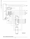
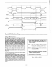
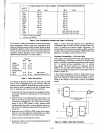
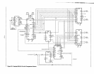
In
more complicated systems where one level of data,
address and
control buffering
is
required (such
as
the case
when there are many
Signal paths and device loading on
one card), the
delays
of
the latches and bidirectional
drivers must be taken into consideration.
First
consider
a ROM, EPROM
or
static
RAM configura·
tion
as shown in Figure
18.
Using
the
generalized
available
memory access formula,
tAD,
tRD
and
tLDR
for
the memory can be determined using
the
data sheet tim-
ing delays
for
the buffers.
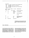
3.125MHz
5MHz
TRD
250 100
TAD
500 275
(BUFFERS)
TLDR
390 200
Figure 18. Medium Buffered System
A1-20