


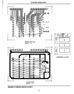
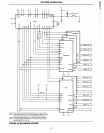


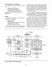
Arithmetic
and Logic
Unit
(ALU):
The
ALU
contains
the
following
registers:
•
An
8-bit
accumulator
•
An
8-bit
temporary
accumulator
(ACT)
• A
5-bit
flag register:
zero,
carry,
sign,
parity
and
auxiliary
carry
• An
8-bit
temporary
register (TMP)
Arithmetic,
logical
and
rotate
operations
are per-
formed
in
the
ALU.
The
ALU
is
fed
by
the
temporary
register (TMP)
and
the
temporary
accumulator
(ACT)
and
carry
flip-flop.
The
result
of
the
operation
can be trans-
ferred
to
the
internal
bus
or
to
the
accumulator;
the
ALU
also
feeds
the
flag register.
The
temporary
register (TMP) receives
information
from
the
internal
bus
and
can send all
or
portions
of
it
to
the
ALU,
the
flag register
and
the
internal
bus.
The
accumulator
(ACC)
can
be
loaded
from
the
ALU
and
the
internal
bus
and
can
transfer
data
to
the
temporary
accumulator
(ACT)
and
the
internal
bus.
The
contents
of
the
accumulator
(ACC)
and
the
auxiliary
carry
flip-flop
can
be
tested
for
decimal
correction
during
the
execution
of
the
DAA
instruction
(see
Section
5).
Instruction Register and
Control:
During an
instruction
fetch,
the
first
byte
of
an
in-
struction
(containing
the
OP
code)
is
transferred
from
the
internal
bus
to
the
8-bit
instruction
register.
The
contents
of
the
instruction
register
are,
in
turn,
available
to
the
instruction
decoder.
The
output
of
the
decoder,
combined
with
various
timing
signals, provides
the
control
signals
for
the
register
array,
ALU
and
data
buffer
blocks. In
addition,
the
outputs
from
the
instruction
decoder
and
external
control
signals feed
the
timing
and
state
control
section
which
generates
the
state
and
cycle
timing
signals.
Data
Bus
Buffer:
This
8-bit
bidirectional
3-state
buffer
is
used
to
isolate
the
CPU's
internal
bus
from
the
external
data
bus
(DO
through
D7). In
the
output
mode,
the
internal
bus
content
is
loaded
into
an
8-bit
latch
that,
in
turn,
drives
the
data
bus
output
buffers.
The
output
buffers
are
switched
off
during
input
or
non-transfer
operations.
During
the
input
mode,
data
from
the
external
data
bus
is
transferred
to
the
internal
bus.
The
internal
bus
is
pre-
charged
at
the
beginning
of
each
internal
state,
except
for
the
transfer
state
(TW
and
T3-described
later
in
this
chapter).
4-3
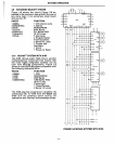
THE PROCESSOR CYCLE
An
instruction
cycle
is
defined
as
the
time
required
to
fetch
and
execute
an
instruction.
During
the
fetch,
a
selected
instruction
(one,
two
or
three
bytes)
is
extracted
from
memory
and
deposited
in
the
CPU's
instruction
regis-
ter.
During
the
execution
phase,
the
instruction
is
decoded
and
translated
into
specific processing
activities.
Every
instruction
cycle
consists
of
one,
two,
three,
four
or
five
machine
cycles. A
machine
cycle
is
required
each
time
the
CPU accesses
memory
or
an
I/O
port.
The
fetch
portion
of
an
instruction
cycle
requires
one
machine
cycle
for
each
byte
to
be
fetched.
The
duration
of
the
execu-
tion
portion
of
the
instruction
cycle
depends
on
the
kind
of
instruction
that
has
been
fetched.
Some
instructions
do
not
require
any
machine
cycles
other
than
those
necessary
to
fetch
the
instruction;
other
instructions,
however,
re-
quire
additional
machine
cycles
to
write
or
read
data
to/
from
memory
or
I/O devices.
The
DAD
instruction
is
an
exception
in
that
it
requires
two
additional
machine
cycles
to
complete
an
internal register-pair
add
(see
Section
5).
Each
machine
cycle
consists
of
three,
four
or
five
states. A
state
is
the
smallest
unit
of
processing
activity
and
is
defined
as
the
interval
between
two
successive positive-
going
transitions
of
the
<1>1
driven
clock
pulse.
The
8080
is
driven
by
a
two-phase
clock
oscillator.
All
processing
activ-
ities
are
referred
to
the
period
of
this
clock.
The
two
non-
overlapping
clock pulses, labeled
<1>1
and
<1>2,
are
furnished
by
external
circuitry.
It is
the
<1>1
clock
pulse
which
divides
each
machine
cycle
into
states.
Timing
logic
within
the
8080
uses
the
clock
inputs
to
produce
a
SYNC
pulse,
which
identifies
the
beginning
of
every
machine
cycle.
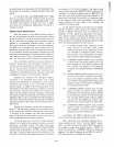
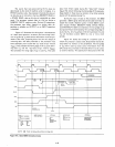
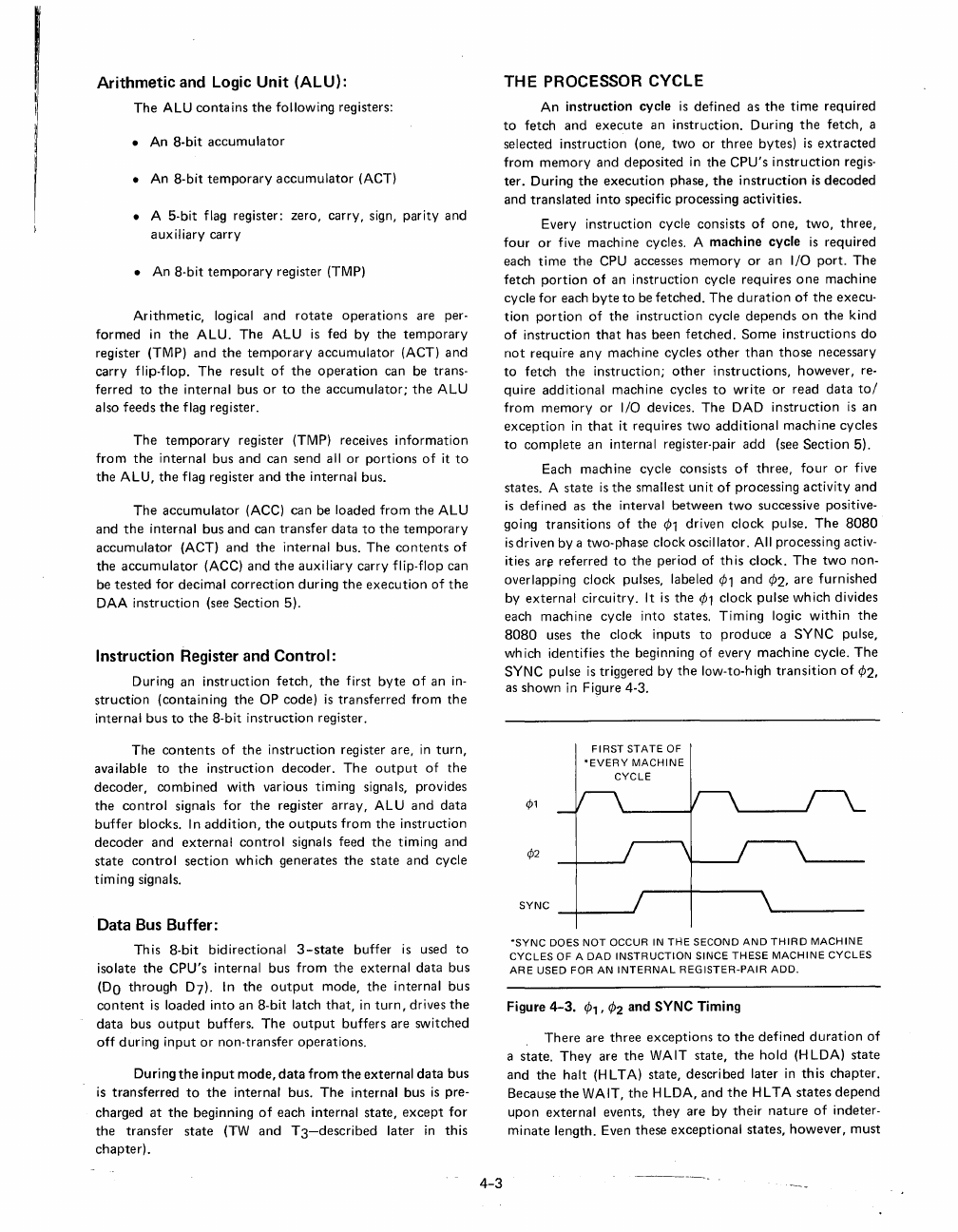
The
SYNC pulse
is
triggered
by
the
low-to-high
transition
of
<1>2,
as
shown
in Figure 4-3.
FIRST
STATE
OF
'EVERY
MACHINE
CYCLE
SYNC
_+-
__
...1
'SYNC
DOES
NOT
OCCUR
IN
THE
SECOND
AND
THIRD
MACHINE
CYCLES
OF
A
DAD
INSTRUCTION
SINCE
THESE
MACHINE
CYCLES
ARE
USED
FOR
AN
INTERNAL
REGISTER-PAIR
ADD.
Figure
4-3.
<1>1,
<1>2
and
SYNC
Timing
There
are
three
exceptions
to
the
defined
duration
of
a
state.
They
are
the
WAIT
state,
the
hold
(H LDA)
state
and
the
halt
(H
L
TA)
state,
described
later
in
this
chapter.
Because
the
WA IT,
the
H LDA,
and
the
H L
TA
states
depend
upon
external
events,
they
are
by
their
nature
of
indeter-
minate
length. Even
these
exceptional
states,
however,
must