


SYSTEM OPERATION
3.3 ADDRESS ASSIGNMENT
3.3.1
Decoding
Besides memory-mapped
I/O, another practice
is
to
only partially decode
the
address bus
when generating
chip
selects. Every device has
a given number
of
unique addresses associated
with
it. The
8355,
for instance, has 2k bytes
of
ROM
and therefore has 2k addresses associated
with
the
ROM.
Anyone
of
these 2k addresses
can be uniquely specified by a pattern on the
11
(211
= 2k) address lines. However, since the 8355
must work with other devices in a system, it
isn't
enough
to
simply specify the
11
bits; fur-
ther
bits
of
information must be used
to
locate
the 2k bytes within the 65k address space. The
2k bytes are located by the use
of
chip enable
(CE)
inputs
to the 8355 chip. If the 8355 were
to
occupy the first 2k bytes
of
the memory address
space,
it
would,
strictly
speaking, be necessary
to
decode the fact
that
A
15
-A
11
were all zeroes,
and use
that
condition as a chip enable. Then
the 8355 would be selected only when the
ad-
dress bus was less than 2k.
However,
if
other 2k blocks
of
addresses aren't
being used, you may combine those addresses
and not decode
all
of
the upper five address
lines
for
chip enables.
In
fact, in a small system
you may need
to
decode only one bit
of
address,
which
is
to
say connect
that
bit
of
the address
bus
to
the chip enable line
of
the 8355.
If
you
connect
A11
to
the
CE
line
of
the 8355 and tie
CE
to
V cc, then the 8355 would be selected when-
ever
the
memory address was less than 2k.
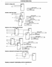
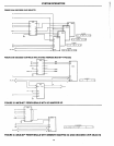
(See
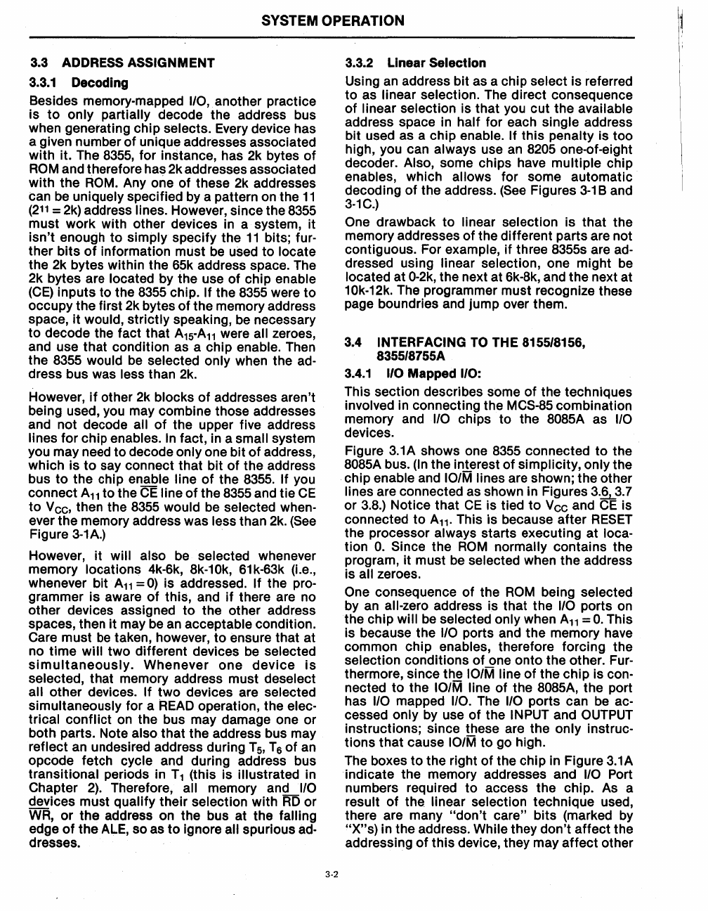
Figure 3-1A.)
However, it
will also be selected whenever
memory locations 4k-6k,
8k-10k,
61
k-63k
(Le.,
whenever bit
A11
=
0)
is addressed. If the pro-
grammer
is
aware
of
this, and
if
there are no
other devices assigned
to
the other address
spaces, then
it
may be an acceptable condition.
Care must
be
taken, however,
to
ensure that
at
no
time
will
two
different devices be selected
simultaneously.
Whenever
one
device
is
selected, that memory address must deselect
all
other
devices. If
two
devices are selected
Simultaneously for a
READ
operation, the elec-
trical
conflict
on the bus may damage one
or
both parts. Note also
that
the
address bus may
reflect an undesired address during T
5
,
T6
of
an
opcode fetch cycle and during address bus
transitional
periods in T 1 (this is illustrated in
Chapter
2).
Therefore, all memory and I/O
devices must
qualify
their selection
with
RD
or
WR,
or
the
address on the bus at the falling
edge
of
the
ALE, so as
to
ignore all spurious
ad-
dresses.
3-2
3.3.2 Linear Selection
Using an address bit as a chip select is referred
to
as linear selection. The direct consequence
of
linear selection is
that
you
cut
the
available
address space in half for each single address
bit used as a chip enable.
If
this
penalty is
too
high, you can always use an 8205 one-of-eight
decoder. Also, some chips have
multiple
chip
enables, which
allows for some automatic
decoding
of
the address.
(See
Figures
3-1
Band
3-1C.)
One drawback
to
linear selection is
that
the
memory addresses
of
the different parts are not
contiguous. For example,
if
three 8355s are ad-
dressed using linear selection, one might be
located
at
0-2k, the next at 6k-8k, and
the
next at
10k·12k. The programmer must recognize these
page boundries and jump over them.
3.4
INTERFACING
TO
THE 8155/8156,
8355/8755A
3.4.1
1/0 Mapped 1/0:
This section describes some
of
the techniques
involved in connecting the
MCS-85 combination
memory and
I/O chips
to
the 8085A as I/O
devices.
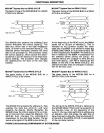
Figure 3.1A shows one 8355 connected
to
the
8085A bus.
(In
the inlerest
of
simplicity, only the
chip enable and
101M
lines are shown; the other
lines are connected as shown in Figures
3.~3.7
or
3.8.) Notice
that
CE
is tied
to
Vcc and
CE
is
connected
to
A
11
. This is because
after
RESET
the processor always starts executing at loca-
tion
O.
Since the
ROM
normally contains the
program, it must be selected when the address
is
all zeroes.
One consequence
of
the
ROM
being selected
by an
all-zero address is that the I/O ports on
the chip
will be selected only when
A11
=
O.
This
is because the
I/O ports and
the
memory have
common
chip
enables, therefore forCing the
selection conditions
of
one onto the other. Fur-
thermore, since
th~
101M
line
of
the
chip
is con-
nected
to
the
101M
line
of
the 8085A, the port
has
I/O mapped I/O. The I/O ports can be ac-
cessed only by use
of
the INPUT and OUTPUT
instructions; since !!lese are the only instruc-
tions
that
cause
101M
to
go high.
The boxes
to
the
right
of
the chip in Figure 3.1A
indicate the memory addresses and
I/O Port
numbers required
to
access
the
chip. As a
result
of
the linear selection technique used,
there are many
"don't
care"
bits
(marked by
"X"s)
in the address. While they
don't
affect
the
addressing
of
this
device, they may
affect
other