


SYSTEM OPERATION
replication
of
bits
Ao-A7).
Assuming
that
memory-mapped
1/0
is used, the addresses are
shown in the boxes to the right in Figure
3-2.
If
you want
to
be sure that neither the
1/0
nor the
memory is ever selected by any
INPUT or
OUT-
PUT
instruction, then the chip enable must
be
conditioned by
101M
=
O.
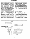
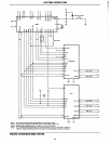
Figure 3.2B shows a somewhat larger system,
also using memory-mapped
1/0.
As in Figure
3.1
B care must
be
exercised
to
ensure that no
two
devices are accessed simultaneously.
You
can see that considerable memory address
space is used up as a result
of
using memory-
mapped
1/0.
3.5
INTERFACING
TO
MCS·80™
PERIPHERALS
3.5.1
1/0 Mapped 1/0:
For want
of
a better name, the Intel® 825x, 827x,
and 829x series peripherals are referred
to
here
as
MCS-80 peripherals because unlike the
81551
56,
8355 and 8755A, they are compatible with
the nonmultiplexed
MCS-80
system bus.
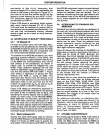
To interface
to
an
MCS-80
peripheral, you must
provide a constant address, a chip select, and
RO
or
WR.
Since the upper address lines
(As-A15)
of
the
8085A are nonmultiplexed, they can be
tied directly
to
the peripherals, as shown in
Figure 3.3A. To provide
1/0 mapped 1/0, use
either
linear selection (keeping the 1/0 and
memory addresses noncoincidental), or condi-
tion the chip selects
WR
with
101M
=
1.
Figure
3.3A shows a
teQ.hnique
of
gating the chip
selects
with
101M
= 1,
using
an 8205.
This
technique also allows more
1/0
devices
to
be
used than
linear selection would. Note that this
technique
relies
on
the fact that the
1/0
Port
number is copied onto
As-A15
as well as
Ao-A7
during an INPUT or OUTPUT instruction.
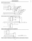
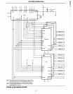
Figure 3.3B shows
an
alternative approach
to
interfacing
to
MCS-80
components.
By
latching
the lower 8 bits
of
address with an
8212,
and
decoding the control signals with an
8205, you
create an exact copy
of
the MCS-80 (8080A,
8224,8228) bus.
You
may then use whatever cir-
cuits
have been previously developed for the
8080. The total cost is one
8212
and one
8205.
Since the same signals might have needed buf-
fering anyway (and the
8212
and 8205 provide
buffering
of
their outputs), the extra component
overhead ranges from
little
to
nothing.
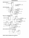
3.5.2 Memory·Mapped
1/0:
Exactly the same techniques used
to
memory
map the
MCS-85
apply to the
MCS-80
1/0
devices.
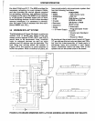
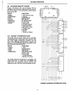
Figure 3.4 shows an
8205 used
to
qualify the
chip select
of
the
110
device with
101M
=
O.
Since
3-5
the
MCS-80
peripherals require nonmultiplexed
address lines, linear select is not too useful
unless the address
lines are latched. This is
because connecting both the chip selects and
the address
lines
of
the
MCS-80
peripherals
to
As-A15
would deplete all the useful addresses
very quickly.
3.6
INTERFACING
TO
STANDARD
BUS
MEMORIES
Standard bus memory devices are designed
to
be used with nonmultiplexed address and data
buses.
Interfacing
to
standard memories is very
similar
to
interfacing to MCS-85 memories with
the exception that
Ao-A7
must be latched. Once
this requirement is met, all the tricks discussed
earlier can
be
used. Since the address lines
would
eventually
require
buffering
as
the
system size grew, the overhead
of
the 8212
latch again becomes negligible.
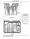
Figure
3.5
shows the interface
of
the 8085A
to
a
large block
of
memory, specifically 16k bytes
of
ROM and
8k
bytes
of
RAM.
Besides
the
memories, the circuit requires only 2-1/6 other
parts for
logical gating. If
MCS-80
1/0
parts were
used, the
8212
latch could be shared between
the two groups, further reducing the gating
overhead per
IC.
Sixteen
2142
chips and eight
2316E
chips are used in
this
deSign. The data
bus, address lines
8-10,
and control signals in
this system
all should be buffered. This applies
to
any system with the number
of
memory
devices represented here.
Wherever
two
or more parts are paralleled on
the same bus, they must be 3-state devices
such as
the
2142 RAM, 2316E ROM, 2716
EPROM,
2332
ROM,
2732
EPROM, and 2364
ROM,
which have either
an
output disable
(00)
input or multiple chip select
(CS)
inputs. To pre-
vent bus contention,
only one memory device
may be output-enabled at a time in this con-
figuration; the
ou~ts
of
all others must be
deselected during
RD.
For additional information
on
interfacing stan-
dard memory devices,
please
read
Section 2
of
Appendix I and the Intel applications note AP-30
"Application
of Intel's
5V
EPROM
and
ROM
Family for Microprocessor Systems" available
from: Intel, Literature Dept.,
3065
Bowers
Ave.,
Santa Clara, CA
95051.
3.7
DYNAMIC
RAM
INTERFACE:
For interfacing the dynamic RAM, Intel makes a
single-component dynamic
RAM
refresh con-
troller, the
8202,
which interfaces the 8085A
to
multiplexed-address-bus dynamic RAMs like