FUNCTIONAL DESCRIPTION
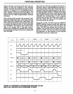
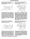
MCS·80™ System Bus
for
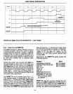
READ CYCLE
The basic timing
of
the
MCS-80
BUS
for
a
READ
CYCLE is as follows:
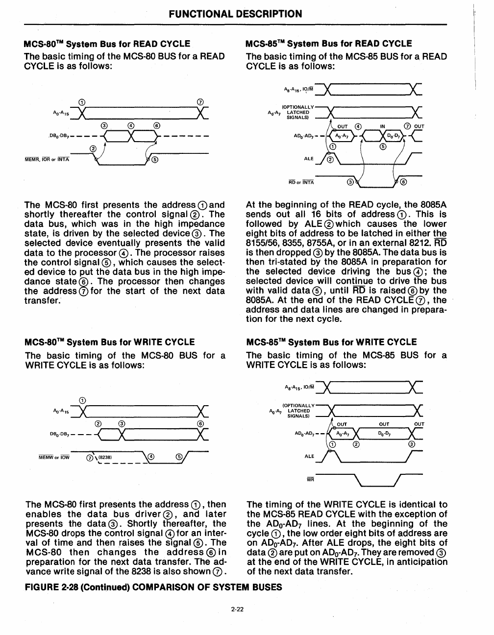
The
MCS-80
first presents the address
CD
and
shortly
thereafter the control signal
®.
The
data bus, which was in the high impedance
state, is driven by the selected device
®.
The
selected device
eventually presents the valid
data
to
the processor
0.
The processor raises
the control signal
®,
which causes the select-
ed
device to put the data bus in the high impe-
dance state
®.
The processor then changes
the address
(])
for the start
of
the next data
transfer.
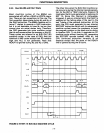
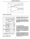
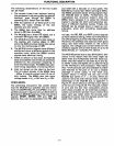
MCS·80™ System Bus
for
WRITE CYCLE
The basic timing
of
the
MCS-80
BUS
for a
WRITE CYCLE is as follows:
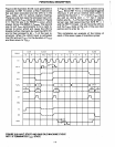
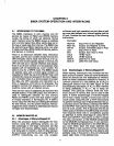
MCS·85™
System
Bus
for
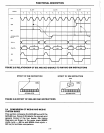
READ CYCLE
The basic timing
of
the MCS-85
BUS
for a
READ
CYCLE is as follows:
Aa-AI5'
IC?/M
==><
__________
>C
(OPTIONALLY=>(
)(
Ao-A7 LATCHED
SIGNALS)
-'---
_____
--<
ALE
Ri5
or
INTA
At the beginning
of
the
READ
cycle, the 8085A
sends out all
16
bits
of
address
CD.
This is
followed by ALE ® which causes the lower
eight bits
of
address
to
be latched in either the
8155/56,8355, 8755A, or in an external 8212.
RD
is then dropped ® by the 8085A. The data bus is
then tri-stated by the
8085A
in
preparation
for
the selected device driving the bus
0;
the
selected device
will continue
to
drive the bus
with
valid data
®,
until
RD
is raised ® by the
8085A. At the end
of
the
READ
CYCLE
(]),
the
address and data lines are changed in
prepara-
tion for the next cycle.
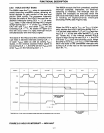
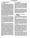
MCS·85™
System
Bus
for
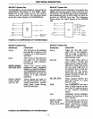
WRITE CYCLE
The basic timing
of
the
MCS-85
BUS
for a
WRITE CYCLE is as follows:
A
S
-A
I5
•
101M
=x'---
______
>C
(OPTIONALLY=>(
)(
Ao-~
LATCHED
SIGNALS)
-------
ALE
WR
The
MCS-80
first
presents the address
CD,
then The timing
of
the WRITE CYCLE is identical
to
enables
the
data
bus
driver
®,
and
later
the
MCS-85
READ
CYCLE with the exception
of
presents the data ®. Shortly thereafter, the the
ADo-AD7
lines.
At
the beginning
of
the
MCS-80 drops the control signal 0 for an inter- cycle
CD,
the low order eight bits
of
address are
val
of
time
and then raises the signal
®.
The on
ADo-AD7'
After ALE drops, the eight bits
of
MCS-80
then
changes
the
address
®
in
data
®are
put on
ADo-AD7'
They are removed ®
preparation for the next data transfer. The ad-
at
the end
of
the WRITE CYCLE, in anticipation
vance write signal
of
the
8238
is also shown
(]).
of
the next data transfer.
FIGURE 2·28 (Continued) COMPARISON
OF
SYSTEM BUSES
2-22


