FUNCTIONAL DESCRIPTION
2.2.4 Arlthmetlc·Loglc Unit (ALU)
The
AlU
contains the accumulator and the flag
register (described in Sections
2.2.1-
and
2.2.2)
and some temporary registers that are inac-
cessible to the programmer.
Arithmetic, logic, and rotate operations are
per-
formed
by
the
AlU.
The results
of
these opera-
tions can
be
deposited in the accumulator, or
they can
be
transferred
to
the internal data bus
for use elsewhere.
2.2.5
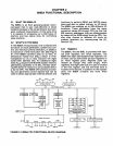
Instruction Register and Decoder
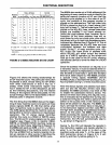
During
an
instruction fetch, the first byte
of
an
instruction (containing the opcode) is trans-
ferred from the internal bus
to
the 8-bit instruc-
tion register.
(See
Figure
2-1.)
The contents
of
the instruction register are, in turn, available to
the instruction decoder. The output of the
decoder, gated by timing signals, controls the
registers,
ALU,
and data and address buffers.
The outputs
of
the instruction decoder and in-
ternal clock generator generate the state and
machine cycle timing signals.
2.2.6
Internal Clock Generator
The
8085A
CPU
incorporates a complete clock
generator on its chip, so
it
requires only the
ad-
dition
of
a quartz crystal to establish timing for
its
operation. (It will accept
an
external clock in-
put at
its
X
1
input instead, however.) A suitable
crystal for the standard
8085A must
be
parallel-
resonant at a fundamental
of
6.25
MHz or less,
twice the desired internal clock frequency. The
8085A-2
will operate with crystal of up to
10
MHz. The functions
of
the 8085A internal clock
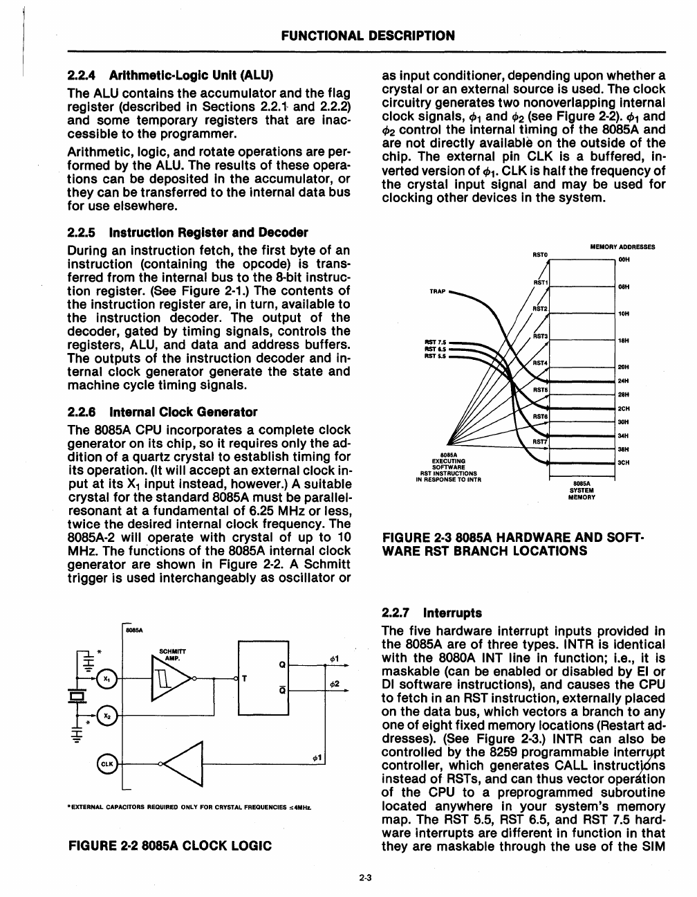
generator are shown in Figure
2-2.
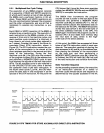
A Schmitt
trigger is used interchangeably as oscillator or
8085A
Q
t----_..-"'_1_
at----_+"'_2_
",1
*EXTERNAL
CAPACITORS REQUIRED ONLY FOR CRYSTAL FREQUENCIES
s4MHz.
FIGURE 2·2 8085A CLOCK LOGIC
2-3
as input conditioner, depending upon whether a
crystal or an external source is used. The clock
circuitry generates two nonoverlapping internal
clock signals,
<P1
and
tP2
(see
Figure
2-2).
<P1
and
<P2
control the internal timing
of
the 8085A and
are not directly
available on the outside
of
the
chip. The external pin
ClK
is a buffered, in-
verted version
of
<P1.
ClK
is half the frequency
of
the crystal input signal and may
be
used for
clocking other devices in the system.
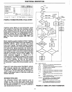
TRAP
lIST
7.5
lIST 1.5
lIST 5.5
MEMORY ADDRESSES
RSTO
r--------,OOH
:J------I08H
..r---------I10H
1-------l18H
.:.i------I20H
~---~28H
~~----I2CH
--I-------I30H
........
-----i34H
~------~~~~----~.H
8085A
EXECUTING
SOFTWARE
RST
INSTRUCTIONS
IN RESPONSE
TO
INTR
--.t---o--i
3CH
8085A
SYSTEM
MEMORY
FIGURE 2·3 8085A HARDWARE AND SOFT·
WARE
RST
BRANCH LOCATIONS
2.2.7 Interrupts
The five hardware interrupt inputs provided in
the
8085A are
of
three types. INTR is identical
with the
8080A INT line in function; i.e.,
it
is
maskable (can
be
enabled or disabled by
EI
or
01
software instructions), and causes the
CPU
to
fetch in
an
RST
instruction, externally placed
on the data bus, which vectors a branch
to
any
one
of
eight fixed memory locations (Restart ad-
dresses).
(See
Figure
2-3.)
INTR can also
be
controlled by the
8259
programmable
inte=r
t
controller, which generates
CAll
instruct" ns
instead
of
RSTs,
and can thus vector oper tion
of
the
CPU
to
a preprogrammed subroutine
located anywhere in your system's memory
map. The
RST
5.5,
RST
6.5,
and
RST
7.5
hard-
ware interrupts are different in function in that
they are maskable through the use
of
the SIM


