


FUNCTIONAL DESCRIPTION
MCS·80™
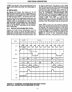
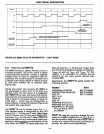
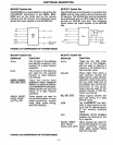
System Bus
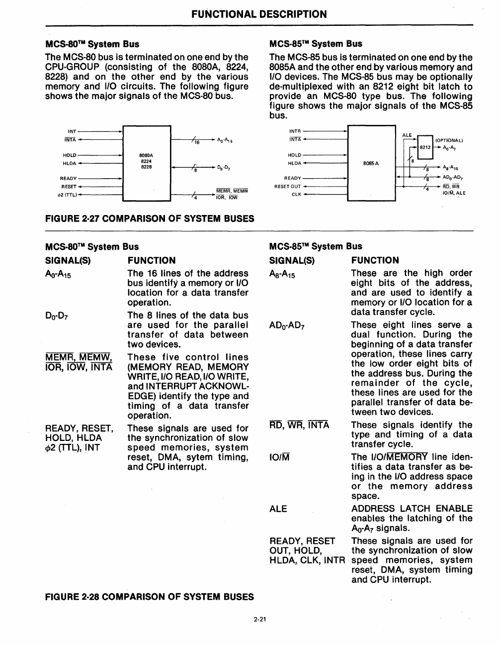
The MCS-80 bus is terminated on one end by the
CPU-GROUP (consisting
of
the 8080A,
8224,
8228)
and on the
other
end by the various
memory and
1/0
circuits. The following figure
shows the major signals
of
the
MCS-80
bus.
INT
INTA
16
Ao-A,s
HOLD
8080A
HlDA
8224
8228
l'
• 0
0
-0
7
i 8
READY
RESET
q,2(TIl)
MEMR, MEMW
lOR,
lOW
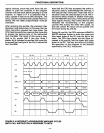
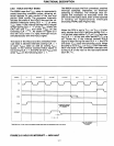
FIGURE 2·27 COMPARISON OF SYSTEM BUSES
MCS·80™
System Bus
SIGNAL(S) FUNCTION
MEMR, MEMW,
lOR, lOW, INTA
READY,
RESET,
HOlD,HlDA
cJ>2
(TTl), I NT
The
16
lines
of
the address
bus identify a memory or
1/0
location for a data transfer
operation.
The 8 lines
of
the data bus
are used
for
the
parallel
transfer
of
data
between
two
devices.
These
five
control
lines
(MEMORY
READ,
MEMORY
WRITE,
1/0
READ,
1/0
WRITE,
and INTERRUPT ACKNOWL-
EDGE)
identify the type and
timing
of
a data transfer
operation.
These signals are used for
the synchronization
of
slow
speed
memories,
system
reset, DMA, sytem timing,
and
CPU
interrupt.
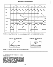
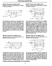
FIGURE 2·28 COMPARISON OF SYSTEM BUSES
2-21
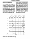
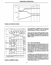
MCS·85™
System Bus
The
MCS-85
bus is terminated on one end by the
8085A and the other end by various memory and
1/0
devices. The
MCS-85
bus may be optionally
de-multiplexed with
an
8212 eight bit latch
to
provide an MCS-80 type bus. The following
figure shows the major signals
of
the MCS-85
bus.
INTR
INTA
HOLD
HlDA
SOS5A
READY
RESET OUT
elK
mEt
,--1
(0
-18212
8
8
8
/
4
A
S
-A
1S
ADo-AD7
RD,WR
101M,
~lE
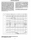
MCS·85™
System Bus
SIGNAL(S) FUNCTION
101M
ALE
These are the high order
eight
bits
of
the address,
and are used
to
identify a
memory or
I/O location for a
data transfer cycle.
These eight lines serve a
dual function. During the
beginning
of
a data transfer
operation, these
lines carry
the low order eight bits
of
the address bus. During the
remainder
of
the
cycle,
these lines are used for the
parallel transfer
of
data
be-
tween
two
devices.
These signals identify the
type and timing
of
a data
transfer cycle.
The
I/OIMEMORY line iden-
tifies a data transfer as
be-
ing
in
the I/O address space
or
the
memory
address
space.
ADDRESS
lATCH
ENABLE
enables the latching
of
the
Ao-A7
signals.
READY,
RESET
These signals are used
for
OUT,
HOLD, the synchronization
of
slow
HlDA,
elK,
INTR speed memories,
system
reset, DMA, system timing
and
CPU
interrupt.