


SYSTEM TIMINGS
808SA
elK-IN
vs.
ClK-OUT
vs. Control Timings
This section shows timing characteristics that
relate the input
clock
to
the
control signals
and
the
output
clock.
These timings
can be treated
as
constants, that
is,
within the normal opera-
tive range of the processor, they are cycle or
SOS5A,
A-2
speed independent.
Be
careful about manipulating the timings given
in
this section
with the specifications
in
the data sheet. The specifications
on
the
SOS5A,
A-2
are
not
mutually exclusive; that
is,
you
can't
add
minimums to minimums and obtain a valid mini-
mum for some other timing parameter. Where the timing
parameter is specified directly, this takes precedence over
any other method
you
come
up
with to find that specification
(through adding
and
subtracting others). This was not done
to
confuse the
user,
but to provide him with the most optimal
timings
for
his system!
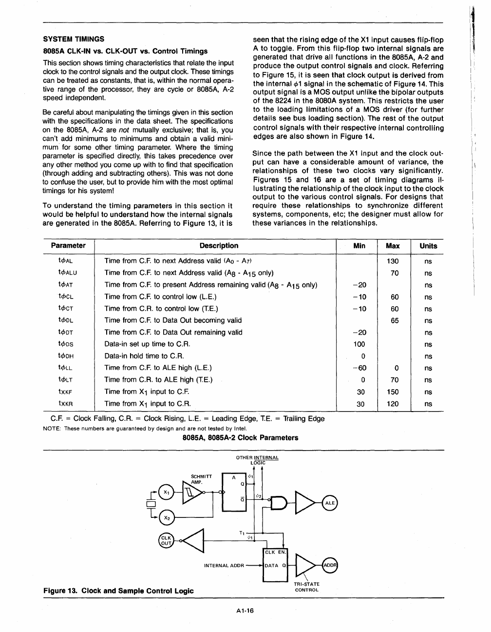
To understand the
timing
parameters in
this
section
it
would
be
helpful
to
understand how the internal signals
are generated in the
SOS5A.
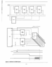
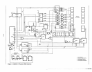
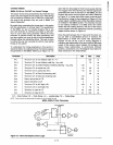
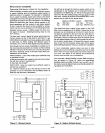
Referring
to
Figure
13,
it
is
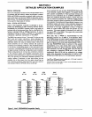
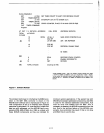
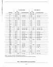
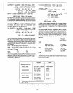
Parameter
Description
t</>AL
Time from
C.F.
to
next Address valid
(Ao
- A7)
seen
that
the rising edge
of
the
X1
input
causes
flip·flop
A
to
toggle. From
this
flip-flop
two
internal signals are
generated
that
drive all functions in
the
SOS5A,
A-2
and
produce
the
output
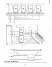
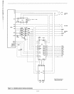
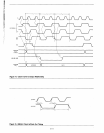
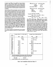
control signals and clock. Referring
to
Figure
15,
it
is seen that
clock
output
is derived from
the internal
<1>1
signal in the schematic
of
Figure 14. This
output
Signal is a MOS
output
unlike
the
bipolar
outputs
of
the
S224
in the
SOSOA
system. This
restricts
the user
to
the loading
limitations
of
a MOS driver (for further
details see bus loading section). The rest
ofthe
output
control signals
with
their
respective internal
controlling
edges are also shown in Figure 14.
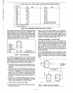
Since
the
path between the
X1
input and
the
clock
out-
put
can have a considerable amount
of
variance, the
relationships
of
these
two
clocks
vary
significantly.
Figures
15
and 16 are a set of
timing
diagrams il-
lustrating
the
relationship
of
the
clock
input
to
the
clock
output
to
the
various control signals. For designs that
require these relationships
to
synchronize
different
systems, components, etc; the designer
must
allow
for
these variances in the rel3tionships.
Min
Max Units
130
ns
t</>ALU
Time from
C.F.
to
next Address valid
(AS
-
A15
only)
70
ns
t</>AT
Time from
C.F.
to present Address remaining valid
(AS
- A15 only)
t</>CL
Time from
C.F.
to control low (L.E.)
t</>CT
Time from
C.R.
to control low
(T.E.)
t</>OL
Time from
C.F.
to Data Out becoming valid
t</>OT
Time from
C.F.
to Data Out remaining valid
t</>os
Data-in
set
up
time to
C.R.
t</>OH
Data-in hold time to
C.R.
t</>LL
Time from
C.F.
to ALE high (L.E.)
t</>LT
Time from
C.R.
to ALE high
(T.E.)
tXKF
Time from X 1 input to
C.F.
tXKR
Time from
X1
input to
C.R.
C.F.
= Clock Falling,
C.R.
= Clock Rising,
L.E.
= Leading
Edge,
T.E.
= Trailing Edge
NOTE: These numbers are guaranteed
by
design and are
not
tested by Intel.
808SA, 808SA-2 Clock Parameters
Figure 13.
Clock
and Sample
Control
Logic
OTHER
INTERNAL
L~
A1-16
TRI-STATE
CONTROL
-20
ns
-10
60
ns
-10
60
ns
65
ns
-20
ns
100
ns
0
ns
-60
0
ns
0
70
ns
30
150
ns
30
120
ns