


CHAPTER 3
SOSSA
SYSTEM OPERATION
AND
INTERFACING
3.1
INTERFACING
TO
THE
8085A
The
8085A
interfaces to both memory and
1/0
devices
by
means
of
READ
and
WRITE
machine
cycles, the timing
of
which are identical. During
each machine cycle the
8085A
issues
an
address
and a control signal, then either sends data out on
the bus or reads data from the bus. The
8085A
may
be performing a READ machine cycle, but what
it
reads could be a ROM, RAM, I/O device, periph·
eral device,
or
nothing.
There is no distinction between data, instruction
opcodes, and
1/0
port numbers except the way the
CPU
interprets what it reads from the bus. If
an
op-
code is what would logically appear on the bus, the
CPU
will treat as
an
opcode whatever does appear
there;
if
an
110
port number is
to
be expected, what
appears will
be
interpreted as a port number. The
same is true for a
WRITE
cycle. The
8085A
issues
an
address, data, and a control signal. Unless it is
requested
to
WAIT
(by
use
of
the
READY
line) it will
complete the
cycle and proceed
to
the next.
Regard-
less of whether there is a device present to accept
the data, the
CPU
executes one instruction at a
time, in sequence, until
told
to
do otherwise.
The
program controls the sequence and nature of all
machine cycles until
an
interrupt occurs.
There are two ways
of
addressing
1/0
devices in the
MCS85 system. If the
101M
output from the
CPU
is
used to distinguish between
1/0
and memory
READ
and
WRITE
cycles, then that system is said
to employ standard, or
I/O-mapped,
1/0.
If
101M
is
not so used, the
CPU
does not distinguish between
1/0
and memory, and its system employs memory-
mapped
1/0.
Each
method
of
addressing
1/0
has
ad-
vantages and disadvantages.
3.2
MEMORY·MAPPED
110
3.2.1
Advantages
of
Memory·Mapped
110
Since the processor doesn't distinguish
110
from
memory using this addressing scheme, you can
take advantage of the larger instruction set that
references the memory address space.
Instead
of
only being able to transfer a byte
of
data between
the accumulator and the
1/0
port (using
INPUT
and
OUTPUT
instructions), you can now program
3-1
arithmetic and logic operations on port data as well
as move data between any internal register and the
1/0
port. Consider the
new
meaning
of
the following
instructions:
Examples:
MOVr,M
MOV
M,r
MVIM
LOA
STA
LHLD
SHLD
ADDM
ANAM
(Input Port
to
any Register)
(Output any Register to Port)
(Output immediate data
to
Port)
(Input Port
to
ACC)
(Output from
ACC
to
Port)
(16-Bit
Input)
(16-Bit
Output)
(Add
Port
to
ACC)
(AN
0 Port with
ACC)
3.2.2
Disadvantages of Memory·Mapped
110
While memory instructions may increase the flex-
ibility
of
the
1/0
system, there are some drawbacks.
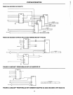
Since
1/0
devices are now addressed as memory,
there are fewer addresses available for memory. A
common practice is to use address bit
15
(A
15
)
to
distinguish memory from
1/0.
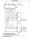
(See
Figure
3-2
and
accompanying discussion.)
If A
15
= 0 then memory
is being addressed; if A
15
=
1,
1/0
is being
ad-
dressed. This particular scheme limits the max-
imum amount
of
memory that can
be
used to 32k
bytes. A further disadvantage
of
memory-mapped
I/O
is
that
it
takes 3 bytes
of
instruction
and
13
clock
cycles using the LOA
or
STA
instructions
to
specify
moving a byte
of
data between
the
ac-
cumulator
and
an
1/0
device, whereas
the
INPUT
and OUTPUT instructions require
only
two
bytes
and
10
clock
cycles. This
is
because
the
I/O ad-
dress space
is
smaller (only 256 bytes) and there-
fore requires fewer bits
to
completely
specify
an address. A
futher
advantage
of
using
the
IN-
PUT
and OUTPUT
Instructions
is
that
it
allows
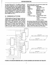
the easy connection of
the
MCS-80 peripherals
to
the
MCS-85 multiplexed bus.
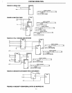
If
you memory-
map
the
MCS-80 peripherals
to
the
MCS-85 bus,
you
must
either
latch
the
lower
address
bits
with
an 8212
or
use a portion
of
the
memory ad-
dress space by connecting
the
chip
selects and
address lines
of
the
ports
to
the
unmultiplexed
upper
eight
lines
of
the address bus.