FUNCTIONAL DESCRIPTION
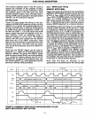
The memory address used in the OF cycle is
always the contents
of
the program counter,
which pOints
to
the current instruction, while
the address used in the
MR
cycle can have
several possible origins. Also, the data read in
during
an
MR
cycle is placed in the appropriate
register, not the instruction register.
110
READ (lOR):
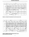
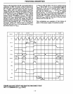
Figure 2-15 also shows the timing
of
two suc-
cessive
I/O
READ
(lOR)
machine cycles, the first
without
aT
WAIT
state. As is readily apparent, the
timing
of
an
lOR cycle is identical to the timing
of
an
MR
cycle, with the exception
of
101M
= 0
for
MR
and
101M
= 1 for lOR; recall that
101M
status signal identifies the address
of
the cur-
rent machine cycle as selecting either a
memory
location or
an
I/O
port. The address
used in the
lOR
cycle comes from the second
byte (Port
No.)
of
an
INPUT instruction. Note
that the
I/O
port address is duplicated onto both
ADo-AD7
and
As-A15.
The
lOR
cycle can occur
only as the third machine cycle of
an
INPUT in-
struction.
Note that the
READY
signal can
be
used to
generate T
WAIT
states for
I/O
devices as well as
memory devices.
By
gating the
READY
signal
with the proper status lines, one could generate
T
WAIT
states for memory devices only or for
I/O
devices only. By gating in the address lines, one
can further
qualify
TWAIT
state generation by the
particular devices being accessed.
MWOR
lOW
81GNAl
T1
T2
T3
2.3.3 WRITE Cycle
Timing
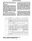
MEMORY WRITE (MW):
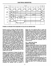
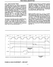
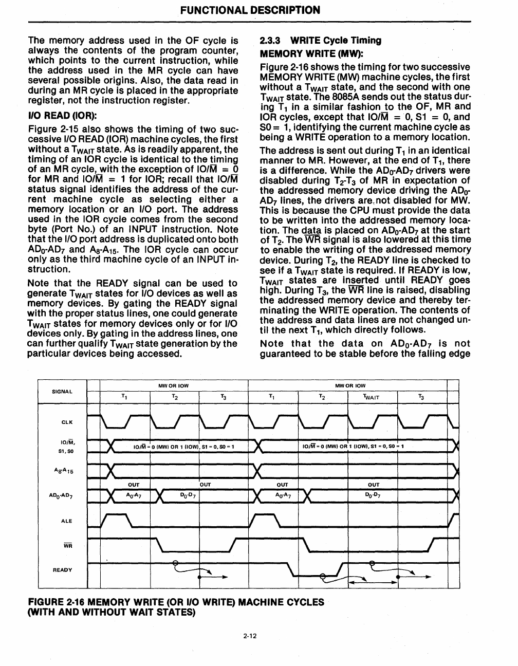
Figure 2-16 shows the timing for two successive
MEMORY
WRITE
(MW)
machine cycles, the first
without a T
WAIT
state, and the second with one
TWAIT
state. The
BOB5A
sends out the status dur-
ing
T1
in a similar fashion
to
the OF,
MR
and
lOR cycles, except that
101M
=0,51
=
0,
and
50
=
1,
identifying the current machine cycle as
being a
WRITE
operation
to
a memory location.
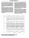
The address is sent out during
T1
in
an
identical
manner
to
MR.
However, at the end of
T1I
there
is a difference.
While the
ADo-AD7
drivers were
disabled during T
2
-T
3
of
MR
in expectation
of
the addressed memory device driving the
ADo-
AD7
lines, the drivers are,not disabled for
MW.
This is because the
CPU
must provide the data
to
be
written into the addressed memory loca-
tion. The data is placed on
ADo-AD7
at the start
of
T 2. The
WR
signal is also lowered at this time
to
enable the writing
of
the addressed memory
device. During T
2, the
READY
line is checked
to
see
if
a T
WAIT
state is required.
If
READY
is low,
T
WAIT
states are inserted until
READY
goes
high. During T
3
,
the
WR
line is raised, disabling
the addressed memory device and thereby ter-
minating the
WRITE
operation. The contents
of
the address and data lines are not changed
un-
til
the next T
11
which directly follows.
Note
that
the
data
on ADo-AD7
is
not
guaranteed to
be
stable before the falling edge
MWOR
lOW
T1
T2
TWA
IT
T3
I--
l..J
l..J l..J
l..J
LI
l..J l..J
~
elK
--
101M,
ex
101M = 0 {MWI
OR
1
{lOWI.81
=
0,
so
= 1
101M = 0 {MWI OR 1
(lOWI,81
=
0,
so
= 1
81,80
I--
I--
P<
A8"A15
~
OUT
OUT
OUT
I--
:x
AD
O
·AD
7
AO-A7
0
0
.0
7
AO·A7
I--
ALE
r-\
1\
I--
WR
,..
READY
C-
~
~
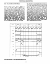
FIGURE 2·16 MEMORY WRITE (OR
110
WRITE) MACHINE CYCLES
(WITH AND WITHOUT WAIT STATES)
2-12
OUT
0
0
.0
7
""(
~
..
)
)
)(
r
r
-
,


