FUNCTIONAL DESCRIPTION
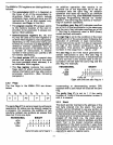
Status &
Buses
Control
Machine
State
S',SO
101M
As-A1S
ADo-AD7
Ro,WR
INTA
ALE
T1
X
X
X X
1 1
1t
T2
X
X
X X X X
0
TWAIT
X
X
X X X X
0
T3
X
X
X X X X
0
T4
1
0*
X
TS
1 1 0
Ts
1
0*
X
TS
1 1 0
Ts
1
0*
X
TS
1
1 0
TRESET
X TS TS
TS
TS 1
0
THALT
0
TS
TS TS TS 1
0
THOLD
X
TS TS TS TS
1 0
O=Logic"O"
1 = Logic
"1"
TS=High
Impedance X=Unspecified
tALE
not generated during 2nd and 3rd machine cycles
of
DAD
instruction.
*IO/iiii = 1 during T
4-
TS states
of
RST
and
INA
cycles.
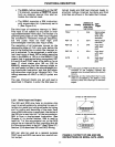
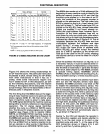
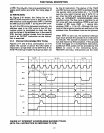
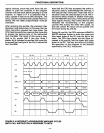
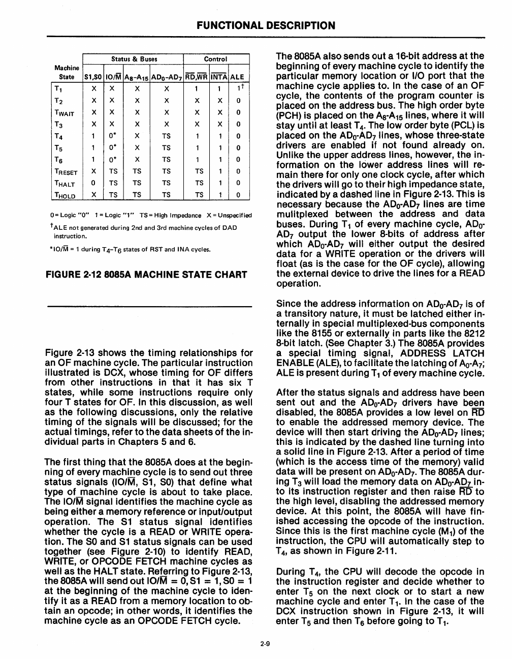
FIGURE 2·12 808SA
MACHINE
STATE CHART
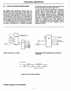
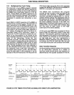
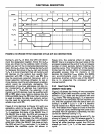
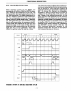
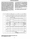
Figure
2-13
shows the timing relationships for
an
OF machine cycle. The particular instruction
illustrated is
DCX,
whose timing for OF differs
from other instructions in that
it
has six T
states, while some instructions require
only
four T states for OF. In
this
discussion, as well
as the following discussions, only the relative
timing
of
the signals will be discussed; for the
actual timings, refer
to
the data sheets
of
the in-
dividual parts in Chapters 5 and
6.
The first thing
that
the
SOS5A
does at the begin-
ning
of
every machine cycle is
to
send out three
status signals
(101M,
S1,
SO)
that
define what
type
of
machine cycle
is
about
to
take place.
The
101M
signal identifies the machine cycle as
being either a memory reference or inputloutput
operation. The
S1
status
signal
identifies
whether the cycle is a
READ
or WRITE opera-
tion. The
SO
and
S1
status signals can be used
together (see Figure
2-10)
to
identify
READ,
WRITE, or OPCODE FETCH machine cycles as
well as the HALT state. Referring
to
Figure
2-13,
the
SOS5A
will send
out
101M
=
0,
S1
=
1,
SO
= 1
at the beginning
of
the machine cycle
to
iden-
tify
it
as a
READ
from a memory location
to
ob-
tain an opcode; in other words,
it
identifies the
machine cycle as an
OPCODE FETCH cycle.
2-9
The
SOS5A
also sends out a 16-bit address at the
beginning
of
every machine cycle
to
identify the
particular memory location or
I/O port
that
the
machine
cycle applies to.
In
the case
of
an OF
cycle, the contents
of
the program counter is
placed on the address bus. The high order byte
(PCH)
is placed on the
A8~A15Iines,
where
it
will
stay until at least T 4. The low order byte (PCl) is
placed on the
ADo-AD7
lines, whose three-state
drivers are enabled if not found already on.
Unlike the upper address lines, however, the in-
formation on the
lower address lines will
re-
main there for only one
clock
cycle, after which
the drivers will go
to
their high impedance state,
indicated by a dashed
line in Figure
2-13.
This is
necessary because the
ADo-AD7
lines are
time
mulitplexed between the address and data
buses. During
T1
of
every machine cycle,
ADo-
AD7
output the lower S-bits
of
address after
which
ADo-AD7
will either output the desired
data for a
WRITE operation or the drivers will
float
(as is the case for the OF cycle), allowing
the external device
to
drive the lines for a
READ
operation.
Since the address- information on
ADo-AD7
is
of
a transitory nature,
it
must be latched either in-
ternally in special multiplexed-bus components
like the
S155
or externally in parts like the
S212
S-bit latch.
(See
Chapter
3.)
The
SOS5A
provides
a special timing signal,
ADDRESS
lATCH
ENABLE
(ALE),
to
facilitate the latching
of
Ao-A7;
ALE is present during
T1
of
every machine cycle.
After the status signals and address have been
sent out and the
ADo-AD7
drivers have been
disabled, the
SOS5A
provides a low level on
RD
to
enable the addressed memory device. The
device
will then start driving the
ADo-AD7
lines;
this
is indicated by the dashed line turning
into
a solid line in Figure
2-13.
After a period
of
time
(which is the access time
of
the memory) valid
data
will
be
present on
ADo-AD7'
The
SOS5A
dur-
ing
T3
will load the memory data on
ADo~A!?Lin
to
its
instruction register and then raise
RD
to
the high level, disabling the addressed memory
device. At this point, the
SOS5A
will have fin-
ished accessing the opcode
of
the instruction.
Since this is the
first
machine cycle
(M
1
)
of
the
instruction, the
CPU
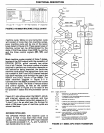
will automatically step
to
T
4
,
as shown in Figure
2-11.
During T
4
,
the
CPU
will decode the opcode in
the instruction register and decide whether
to
enter T 5 on the next clock or
to
start a new
machine cycle and enter T
1
.
In the case
of
the
DCX
instruction shown in Figure
2-13,
it
will
enter
T5
arid then
T6
before going
to
T
1
.


