


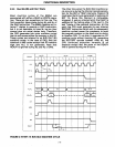
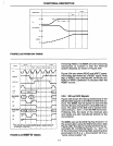


FUNCTIONAL DESCRIPTION
The following observations
of
the two buses
can be made:
1.
The access times from address leaving
the processor
to
returning data are almost
identical, even though the
SOS5A
is
operating
50% faster than the
SOSO.
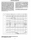
2.
With the addition
of
an
S212
latch to the
SOS5A,
the basic timings
of
the
two
systems are very similar.
3.
The
SOS5A
has more time for address
setup
to
FfO
than the
SOSO.
4.
The
MCS-SO
has a wider
RD
signal, but a
narrower
WR
signal than the
SOS5A.
5.
The
MCS-SO
provides stable data setup
to
the leading and trailing edges
of
WR,
while the
SOS5
provides stable data setup
to
only the trailing edge
of
WA.
6.
The
MCS-SO
control signals have different
widths and occur at different points in the
machine cycle, while the
S085A
control
signals have identical timing.
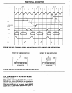
7.
While not shown on the chart, the
MCS-SO
data and address hold times are adversely
affected by the processor preparing
to
enter the HOLD state. The
SOS5A
has iden-
tical timing regardless
of
entering HOLD.
S.
Also not shown on the chart is the fact
that
all output signals
of
the
80S5A
have
- 400l'a
of
source current and
2.0
rna
of
sink current. The
SOS5A
also has input
voltage levels
of
V
1L
=
O.SV
and V
1H
= 2.0V.
CONCLUSION:
The preceding discussion has clearly shown
that
the
MCS-S5
bus satisfies the two restric-
tions
of
COMPATIBILITY and
SPEED.
It is com-
patible because
it
requires only an
S212
latch
to
generate an
MCS-SO
type
bu~f
the four control
signals MEMR, MEMW,
lOR and lOW are
desired, they can be generated from
RD,
WR,
2-23
and
101M
with a decoder or a few gates. The
MCS-85 bus is also fast. While running at 3MHz,
the
SOS5A
generates better
timing
signals than
the
MCS-80
does at
2M
Hz.
Furthermore, the
multiplexed bus structure doesn't slow the
SOS5A
down, because
it
is using the internal
states
to
overlap the fetch and execution por-
tions
of
different machine cycles. Finally, the
MCS-S5
can be slowed down
or
sped up con-
siderably,
while
still
providing
reasonable
timing.
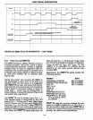
TO
USE.
The
AD,
WR, and INTA control signals
all have identical timing, which
isn't
affected by
the
CPU
preparing
to
enter the HOLD state. Fur-
thermore, the address and data bus have good
setup and hold times relative
to
the control
signals. The voltage and current levels for the
interface signals will all drive buses
of
up
to
40
MOS devices, or 1 schottky
TIL
device.
The
MCS-S5
system bus is also EFFICIENT. Effi-
ciency is the reason that the lower eight ad-
dress lines are multiplexed with the data bus.
Every chip that needs to use both
Ao-A7
and 0
0
-
0
7
saves 7 pins (the eighth pin is used for ALE)
on the interface
to
the processor. That means
that
7 more pins per part are available
to
either
add features
to
the part
or
to
use a smaller
package in some cases.
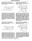
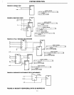
In
the three chip
system shown in Figure
3-6,
the use
of
the
MCS-S5
bus saves 3 x 7 =
21
pins, which are
used for extra
I/O
and interrupt lines. A further
advantage
of
the
MCS-S5
bus is apparent in
Figure
3-7,
which shows a printed
circuit
layout
of
the circuit in Figure
3-6.
The reduced number
of
pins and the fact
that
compatible pinouts
were used, provides for an extremely compact,
simple, and efficient printed circuit. Notice that
great care was taken when the pinouts were
assigned
to
ensure that the signals would flow
easily from chip
to
chip
to
Chip.