


FUNCTIONAL DESCRIPTION
M,(OF)
POWER
SUPPLY
TRESET
T,
T,
+5V
.~
4.7SV
Vee
.7J==->
10ms.c
-
OV
Vaa
(INTERNAL)
-2V.1-
2.4V
...
RESET
IN
OV.
..
_----
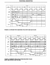
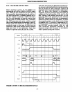
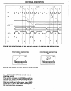
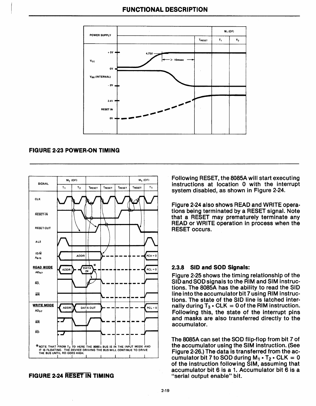
FIGURE 2·23 POWER·ON TIMING
SIGNAL
ClK
RESET
OUT
ALE
101M
As-!s
READ MODE
ADo.7
RD,
WRITE MODE
ADo.7
..........
*NOTE
THAT
FROM T2 TO HERE THE 808S's BUS IS IN THE INPUT MODE AND
IT
IS
FLOATING. THE DEVICE DRIVING THE BUS
WILL
CONTINUE TO DRIVE
THE
BUS
UNTIL
RD
GOES
HIGH.
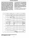
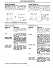
FIGURE 2·24
RESET
IN TIMING
,,-"-
2·19
,,-~
~
,,-"-
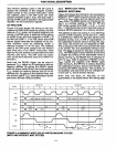
Following
RESET,
the
SOS5A
will
start
executing
instructions at location
0
with
the interrupt
system disabled, as shown in Figure
2-24.
Figure
2-24
also shows READ and WRITE opera-
tions being terminated by a RESET
signal. Note
that
a
RESET
may prematurely terminate any
READ
or
WRITE operation In process when the
RESET
occurs.
2.3.8
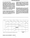
SID and SOD Signals:
Figure
2-25
shows the
timing
relationship
of
the
SID and SOD signals
to
the RIM and SIM instruc-
tions. The
SOS5A
has the
ability
to
read the SID
line
into
the accumulator
bit
7 using
RIM
instruc-
tions. The state
of
the SID line is latched inter-
nally during T 3 •
elK
= 0
of
the
RIM instruction.
Following this, the state
of
the
interrupt pins
and masks are
also transferred directly
to
the
accumulator.
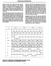
The
SOS5A
can set the
SOD
flip-flop from
bit
7
of
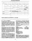
the accumulator using the SIM instruction.
(See
Figure
2-26.)
The
data
is transferred from the ac-
cumulator
bit
7
to
SOD during
M1
• T
2
•
elK
= 0
of
the instruction following SIM, assuming
that
accumulator
bit
6 is a
1.
Accumulator bit 6 is a
"serial output enable" bit.