


STATIC
MEMORIES
The same consideration must be applied to standard static
memories as with the
ROMs/EPROMs in
an
unbuffered sys-
tem. Memory device
selection must
be
qualified
by
a memory
read or write to prevent spurious
selection. Some Intel static
RAM devices have
an
Output Enable for this purpose, such
as the
2142
(1k
x
4).
This part was designed to be specifically
used with a microprocessor bus. For other standard static
RAMs, the chip
selects must be qualified by
RD,
WR
or ALE
to prevent random
selection.
DYNAMIC
RAM INTERFACE
An earlier Intel Application Report (APR-1) extensively cov-
ered dynamic RAM interface with different types of memory
and refresh
in
the MCS-80 system. This dynamic
RAM
section
was taken from the most memory intensive
example
in
APR-1,
the
2116,
modified
to
be compatible with the 808SA bus.
These minor modifications are such that
an
S080 system can
be converted without much
trouble. Before discussion of this
section, however, a strong word of advice is
in
order. At
about the same time this
Application Note is published, Intel
will
be sampling
an
8202 dynamic RAM refresh controller
which does all dynamic RAM interfacing (except the data
bus) and refreshing
in
one packaged component.
It
is highly
recommended that the reader investigate this before using
the attached schematic. Reading this section
will still
be
use-
ful
in
terms of understanding the
80SSA
bus.
This section uses the
APR-1
2116
(multiplexed address 16K)
example modified for the 2117-4 dynamic
RAM.
These
devices
have
some differences from the
2116.
One
is
that the
output
is
not latched and is 3-stated during a write operation.
This
allows a user to tie both the data in and data out pins
together
at the device and
at
the data buffers, saving board
traces. The
2117
also have hidden refresh capabilities where
if
CAS
is
held low,
RAS
can
be
toggled to refresh the device.
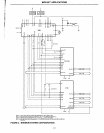
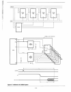
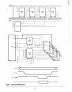
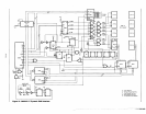
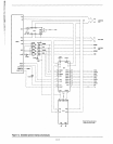
The
schematic
shown
in Figure
10
is
aimed at a
high
performance, relatively
inexpensive
solution
(disregard-
ing
the
S202).
Refresh
circuitry
is
not
shown,
but
can be
implemented
in a
variety
of
ways. This
will
be
discussed
later
in an
upcoming
section.
In
this
refresh
section,
code
for
a
simple,
very
low
cost
refresh
controller
that
requires no
special
hardware,
other
than
an 8155 timer,
is presented.
For system timing, a 4x
clock is used
to
obtain the resolution
necessary to provide the clocks for the multiplexed address
2117's.
Other solutions are possible with delay lines, one
shots, etc., but are
relatively expensive and don't provide for
a nice baud rate source for any
peripherals that may be in the
system as does this 4x
clock. Another approach can use the
clock edges from the
S08SA
CLKOUT
to
interface to dynamic
RAM.
To
facilitate this type of approach, Clock related timing
parameters are
listed later
in
this note.
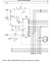
To
aid
in
understanding the operation of this circuit, the ex-
planation is broken into a discussion of the main signal paths.
2117-4
Spec compatibility with the
80S
SA
will
be
discussed
in
detail
in
the dynamic RAM section of the Memory Compatibil-
ity section.
A1-11
Addresses
The
lower
14
addresses
(AO-A13)
are used to select one of
the 16,384 8-bit bytes in each 16K byte data bank. The
lower
8 of these
14
addresses
(AO-A7)
flow through an 8212 and
are
latched by ALE, effectively demultiplexing the address/
data bus. These
lower 8 addresses with the next 6 (AS-A13)
enter the 3242
multiplexer/refresh controller. The Row Enable
of the 3242 controls which half of the addresses are presented
to the dynamic RAM memory. Looking at the row
enable on
the 3242, it is seen that the row
and
column addresses are
swapped with respect to
convention.· The higher order ad-
dresses are used as row addresses and the
lower order
addresses are used as
column addresses. This does not
create
problems because this is invisible to the CPU. Re-
freshing is done
properly as the 3242 controls the addressing
for this. The upper two address
lines
(A14-A,s)
are decoded to
qualify one of the four RAS (Row Address Strobe) lines to
select one of the four 16K byte data banks
of
memory.
Cycle Requests
Cycle requests are generated from several sources; ALE
automatically initiates a request when
S1
indicates that there
is a read taking
place (flip-flop C),
WR
during write cycles (D)
and refresh
delayed
(Q
output of refresh flipflop (B)) when
there is a refresh. ALE is used to
starfa
read (qualified by
S1)
to provide ample time for access from the memories. This
cycle request signal (A) immediately creates a RAS and
starts a timing chain (74S174
shift register ,(E)) to generate
the remaining
signals. Synchronization between this cycle
request pulse and the 4x clock is accomplished by the first D
flip-flop in the 'S174 shift register (timing chain).
RAS/CAS
When RAS is enabled by a cycle request, it is qualified with
either a refresh request
(all RAS's turn on) or the decoded
upper two bits of the address bus. A
careful reader may
question whether address
is
valid prior to RAS being enabled.
This question can be answered
by
noting that the
8212
passes
the address through before the
falling edge of ALE latches it.
TALt
(115
ns
for 320
ns
808SA processor cycle), which is the
time from address to the
falling edge of ALE, gives ample
time for addresses to be valid at the 3242 outputs before
RAS is
valid. RAS is extended past the clearing of the cycle
request flip-flop by ORing this enabling signal with a tap from
the D
flip-flop shift register.
CAS (Column Address Strobe) is produced between
123
and
164 ns after RAS, depending upon when the first D
flip-flop in
the shift register synchronizes with the cycle request
signal
(C). Since this is greater than the specified maximum delay
from RAS to CAS, this memory system is CAS access limited
and RAS access no longer has any meaning. The CAS tap
can't move up one D
flip-flop to provide more time for memory
access as this
would not provide sufficient data set up time
with respect to
CAS during a write.
t Note that TAL now only applies to the high order address byte. TALL, for the
lower address byte equals 90 ns, This was done to allow for additional T RAE
time for data
float.