


FUNCTIONAL DESCRIPTION
M1
(OF)
M1
(OF)
M1
(OF)
SIGNAL
T1
T2
T3
T4
T1
T2 T3
T4
Tl
T2
T3
T4
CLK
V V
</
V
V
V
V V
V
;-
1\/
V
4~
SOD
4~
/
I
~
(
4~
SID
1\
~
\
ACCUMULATOR
W
"-
(BIT7)
A
B
-A
15
~
K=
~
LX
K=
OUT
IN
OUT
IN
OUT
IN
ADO-AD7
C
-(
RIM
I}---
C
~-{
SIM
~--
rc
~-
RIM
I}----
ALE
V\
V\
V\
AD
1\
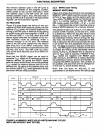
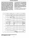
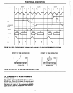
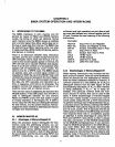
FIGURE 2·25 RELATIONSHIP OF SID AND SOD SIGNALS TO RIM AND SIM INSTRUCTIONS
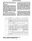
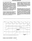
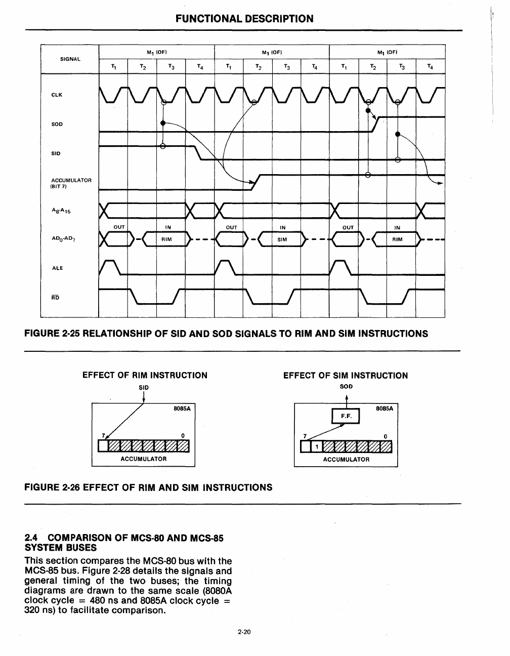
EFFECT OF RIM INSTRUCTION
SID
FIGURE 2·26 EFFECT OF
RIM
AND SIM INSTRUCTIONS
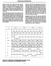
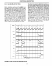
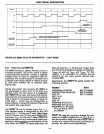
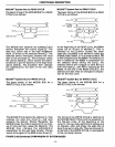
2.4 COMPARISON OF MCS·80 AND MCS·85
SYSTEM BUSES
This section compares the MCS-80 bus
with
the
MCS-85 bus. Figure
2-28
details the signals and
general timing
of
the
two
buses; the timing
diagrams are drawn
to
the same scale (8080A
clock
cycle =
480
ns and 8085A clock cycle =
320
ns)
to
facilitate comparison.
2-20
EFFECT OF SIM INSTRUCTION
SOD