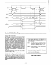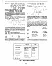
tAD MEMORY = tAD8085A - (8282 + 8205 delay) - (8286
delay) + transitional gain due to buffering*
= tAD85 - (TIVOV + t--) - (TIVOV) + tCAPB *
= (5/2+N)T - 225 -
55
- 35 +
15
=
(5/2+
N)T -
300
(for
8085A)
(5/2+N)T
- 225
(for
8085A-2)
where N = number of wait states and T = cycle time,
For minimum 8085A timing 500ns = tAD memory
8085A-2 timing 275ns
= tAD memory
The 8085A timing parameter tAL was not taken into consider-
ation as the 8282 transfers information directly through with-
out concern of the address latch enable. tRD can be obtained
in a similar manner.
The read signal
RD
goes through a buffer before it reaches
the memory. This must be taken into consideration when
calculating effective tRD for the memory.
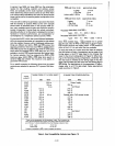
tRD MEMORY = tRD 8085A - (buffer delay) - (8286
delay) + transitional gain due to buffering
= tRD 85 - (delay) - (TIVOV) + tCAPB
= (3/2+N)T -
180
- 30 - 35 +
15
(3/2+
N)T -
230
(for
8085A)
(3/2 + N)T - 200 ns (for 8085A-2)
'tCAPB
is additional time thrown back in for improvement in signal transi-
tions. This is because buffering the signals reduces the capacitive loading
considerably. The data sheet gives timings for maximum capacitive loading.
Characterization has shown change in delay versus capacitive loading
as
.12
nslpf min (under
20
pF loading)
and
.24 ns/pF max (under 150
pF
loading).
To
take into consideration the effects of this loading two param-
eters are defined:
tCAPA - delay for a signal
to
leave the
old
logic level
tCAPS
- delay for a signal
to
complete the transition from
the
old
to new
logic
level
where tCAPA = 1/2 tCAPB
MIN
MAX
tCAPA
tCAPB
7
ns
15
ns
15
ns
30
ns
In the memory compatibility calculations tCAPB
min
is added
on
as
spec sheet
values assume
150
pF loading
and
this system
is
not worst case, i.e., it has
buffering that reduces this loading to approximately 20
pf.
Since the
CAP
=
130 pF and change in delay versus capacitance is 1/2 ns/pF
min,
tCAPSMIN =
(.1
ns/pF) 130
pF
= approx.
15
ns.
MINIMUM SYSTEM:
For minimum 8085A timing
8085A-2 timing
250ns
= tRD memory
100ns = tRD memory
Therefore for tLDR:
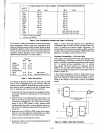
tLDR MEMORY = tLDR 8085 - (buffer delay) - (8205)
- (8286) + tCAPB
=
tLDR-(delay)-(t--)-(TIVOV)+tCAPB
= 2T
-180
-30
-20
-35
+15
= 2T - 250 for 8085A
= 2T
-200
for 8085A-2
For minimum 8085 timing
8085A-2 timing
= 390ns
= 200ns
To
obtain memory access parameters for a multicard system
(which would have buffering at both ends of the system bus),
it is a simple matter of subtracting off the additional buffering
delays.
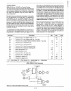
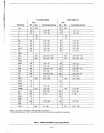
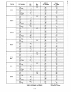
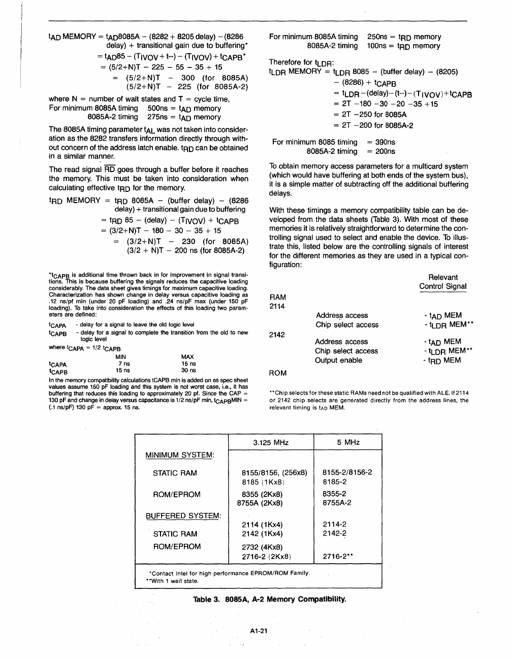
With these timings a memory compatibility table can be de-
veloped from the data sheets
(Table
3). With most of these
memories it is relatively straightforward to determine the con-
trolling signal used to select and enable the device.
To
illus-
trate this, listed below are the contrOlling signals of interest
for the different memories as they
are
used in a typical con-
figuration:
RAM
2114
2142
ROM
AddreS?
access
Chip select access
Address access
Chip select access
Output enable
Relevant
Control Signal
- tAD MEM
- tLDR MEM**
-tAD
MEM
- tLDR MEM**
- tRD MEM
"Chip
selects for these static RAMs need not
be
qualified with ALE. If 2114
or
2142
chip selects are generated directly from the address lines, the
relevant timing
is
tAD
MEM.
3.125
MHz
5 MHz
STATIC
RAM
8155/8156, (256x8)
8155-2/8156-2
8185
(1
Kx8)
8185-2
ROM/EPROM
8355 (2Kx8)
8355-2
8755A (2Kx8)
8755A-2
BUFFERED SYSTEM:
2114 (1Kx4)
2114-2
STATIC
RAM
2142
(1
Kx4)
2142-2
ROM/EPROM
2732 (4Kx8)
2716-2 (2Kx8)
2716-2**
'Contact
Intel
for
high performance EPROM/ROM Family.
"With
1 wait state.
Table 3.
BOSSA,
A-2
Memory Compatibility.
A1-21


