SYSTEM OPERATION
the Intel 2104A and
2117.
The 8202 provides the
necessary refreshing for such dynamic RAMs,
and
also
provides
the
control signals required
for
accessing, selecting, and address clocking.
It
allows
for
the
use
of
the 8085A's full capabili-
ty
of
64k bytes
of
address space
with
no addi-
tional
buffering devices. As
with
other standard
memory interfaces,
it
is necessary
to
demulti-
plex
the
lower 8
bits
of
address from
the
multi-
plexed 8085A
bus,
AD
o
-
7
•
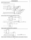
3.8 MINIMUM MCS-85™ SYSTEM
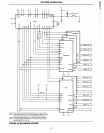
The Schematics
of
Figure 3.6
depict
a minimum
system core.
In actual use, some
of
the pro-
cessor control signals (TRAP, INTR, and HOLD)
would
have
to
be terminated. Also, interface
logic
to
external
devices
as
well
as
more
memory and
1/0
devices may be desirable. The
first
thing
one notices about
the
system in
Figure 3.6 is the
scarcity
of
parts required
to
build
this
system. With a minimum
of
parts, we
have
constructed
a
microcomputer
system
that
has
the
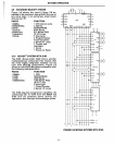
following functions:
PARTS
FUNCTIONS
1 8085A 1 CPU (Clock cycle
1 8355/8755A
:s
320 ns)
1 8156
2048 Bytes
of
either
1
Crystal
4 Resistors
1 Capacitor
1 Diode
1
+ 5 Power Supply
EPROM
or
ROM
256 Bytes
of
RAM
38110
Lines
5
Interrupts
1 Programmable Timerl
Counter
1
Crystal and
Oscillator
1
Clock
1 Power-on Reset
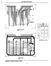
By
looking at
the
printed
circuit
layout
of
Figure
3.7, we can see
that
not
only
are there
just
3 ICs,
but
that
the
interconnection
of
these
p-arts
is
extremely
easy
and
provides
a very
dense
layout. Expecially notice the easy
flow
of
the
system bus on
the
solder side
of
the board.
2 X 2142
WR
A13
A"
All
Vee
A,s
101M
AD
o
·AD
7
Vee
ALE
As"A
1O
RD
A"
----------_~---ICS2
,.------t-------QCSI
CS2
,..-------<l
CSI
---------~~-----~~
OD
8205
A,
0,
A
g
,9
A,
Ao
2 X 2142
=0 /
/
/
2316E
E,
t-+------<lCSl
E,
t------<lCS2
E,
0
0
8212
Ao·A?
01
1
_
8
00
1
.
8
MD
I
STB
I
DS,
=0 /
DS
1
=7
I
/
/
=7
/
/
/
MEMORY ADDRESS
/11
0 1 1 1 I 1 X
A.
I-
I
I
/
/
MEMORY
ADDRESS
/
/
/
MEMORY ADDRESS
/ 1 0 0 1 1 I 1
AlO
- - I
/
MEMORY
ADDRESS
I 0 0 0 0 I 0
AlO
- - I -I -
-
I-
Ao
I
/
Ao
1/
/
/
/
-I -
Ao
Ao
i/
/
I
/
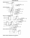
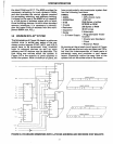
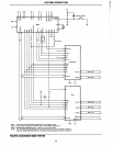
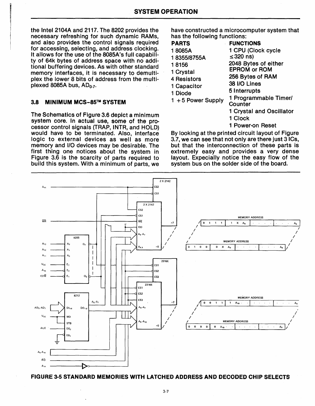
FIGURE 3·5 STANDARD MEMORIES WITH LATCHED ADDRESS AND DECODED CHIP SELECTS
3-7


