


CHAPTER 2
SOSSA
FUNCTIONAL DESCRIPTION
2.1
WHAT
TH
E 808SA IS
The 8085A is
an
8-bit general-purpose micro-
processor that is very cost-effective in small
systems because
of
its
extraordinarily low hard-
ware overhead requirements. At the same time
it is
capable of accessing up
to
64K bytes
of
memory and has status lines for controlling
large
systems.
2.2 WHAT'S IN THE 808SA
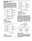
In
the 8085A microprocessor are contained the
functions
of
clock generation, system bus con-
trol,
and interrupt priority selection, in addition
to
execution
of
the instruction set.
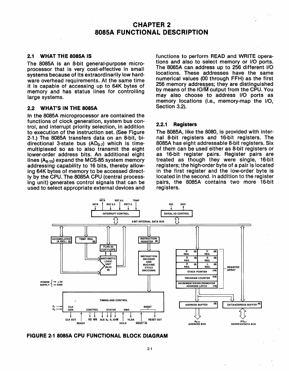
(See
Figure
2-1.)
The 8085A transfers data on
an
8-bit, bi-
directional
3-state bus
(AD
o
-
7
) which is time-
multiplexed
so as
to
also transmit the eight
lower-order address bits. An additional eight
lines
(A
a
.
15
) expand the MCS-85 system memory
addressing capability
to
16
bits, thereby allow-
ing 64K bytes
of
memory to be accessed direct-
ly
by the
CPU.
The 8085A
CPU
(central process-
ing unit) generates control signals that can
be
used to select appropriate external devices and
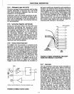
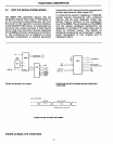
POWER{-+5V
SUPPLY
_GND
X,
X
2
INTA
RST6.5
TRAP
.s TIMING AND CONTROL
functions
to
perform
READ
and WRITE opera-
tions and also
to
select memory or
1/0
ports.
The
8085A can address up
to
256
different
1/0
locations. These addresses have the same
numerical values
(00
through FFH) as the first
256
memory addresses; they are distinguished
by means
of
the
101M
output from the
CPU.
You
may
also choose
to
address
1/0
ports as
memory
locations
(Le.,
memory-map the
1/0,
Section
3.2).
2.2.1
Registers
The 8085A, like the
8080,
is provided with inter-
nal
8-bit registers and 16-bit registers. The
8085A has eight addressable 8-bit registers. Six
of
them can be used either
~s
8-bit registers or
as 16-bit register pairs. Register pairs are
treated as though they were
single, 16-bit
registers; the high-order byte
of
a pair is located
in the first register and the low-order byte is
located in the second.
In
addition
to
the register
pairs, the
8085A contains two more 16-bit
registers.
B
(8)
C (8)
REG.
REG.
D
(8)
E (8)
REG.
REG.
H
(8)
L (8)
REG.
REG.
STACK
POINTER
(16)
PROGRAM
COUNTER
(16)
As-,s
ADDRESS
BUS
REGISTER
ARRAY
AD
o
•
7
ADDRESSIDATA
BUS
FIGURE
2·1
808SA
CPU
FUNCTIONAL BLOCK DIAGRAM
2-1