


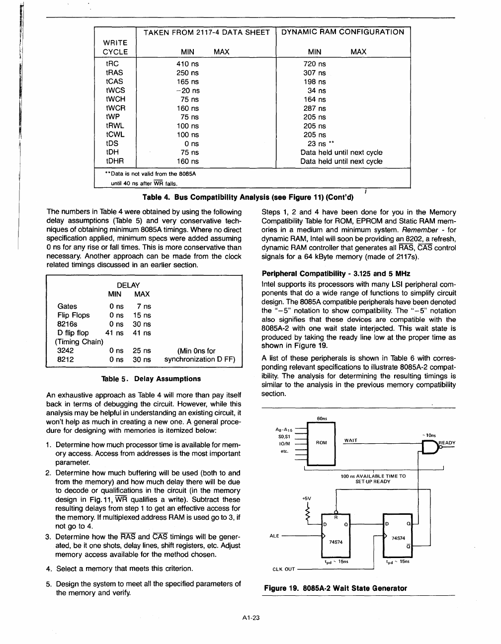
TAKEN FROM 2117-4
DATA
SHEET
DYNAMIC
RAM
CONFIGURATION
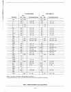
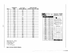
WRITE
CYCLE MIN
MAX
MIN
MAX
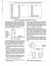
tRC
410
ns
720
ns
tRAS
250
ns
307
ns
tCAS
165
ns
198
ns
tWCS
-20
ns
34 ns
tWCH
75
ns
164
ns
tWCR
160
ns
287
ns
tWP
75
ns
205
ns
tRWL
100
ns
205
ns
tCWL
100
ns
205
ns
tDS
o
ns
23
ns
••
tDH
75
ns
Data held until next cycle
tDHR
160
ns
Data held until next cycle
••
Data is not valid from the 8085A
until 40
ns
after
WR
falls.
I
Table
4.
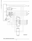
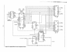
Bus Compatibility Analysis (see Figure 11) (Cont'd)
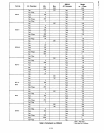
The numbers
in
Table
4 were obtained by using the following
delay assumptions
(Table
5)
and very conservative tech-
niques of obtaining minimum 8085A timings. Where
no
direct
specification applied, minimum specs were added assuming
o
ns
for any rise or fall times. This is more conservative than
necessary. Another approach can be made from the clock
related timings discussed
in
an
earlier section.
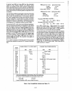
DELAY
MIN MAX
Gates o
ns
7
ns
Flip Flops o
ns
15
ns
8216s o
ns
30
ns
D flip flop
41
ns
41
ns
(Timing Chain)
3242
o
ns
25
ns
(Min
Ons
for
8212
o
ns
30
ns
synchronization D
FF)
Table 5. Delay Assumptions
An exhaustive approach as
Table
4 will more than pay itself
back
in
terms of debugging the circuit. However, while this
analysis may be helpful
in
understanding
an
existing circuit, it
won't help as much
in
creating a new one. A general proce-
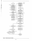
dure for designing with memories is itemized below:
1.
Determine how much processor time is available for mem-
ory access. Access from addresses is the most important
parameter.
2.
Determine how much buffering will be used (both to and
from the memory) and how much delay there will be due
to decode or qualifications
in
the circuit (in the memory
design in Fig.
11,
WR qualifies a write). Subtract these
resulting delays from step 1 to get
an
effective access for
the memory.
If multiplexed address RAM is used go to
3,
if
not go to
4.
3. Determine how the
RAS
and CAS timings will be gener-
ated, be
it
one shots, delay lines, shift registers, etc. Adjust
memory access available for the method chosen.
4.
Select a memory that meets this criterion.
5.
Design the system to meet
all
the specified parameters of
the memory and verify.
A1-23
Steps
1,
2 and 4 have been done for you
in
the Memory
Compatibility Table for ROM, EPROM and Static RAM mem-
ories
in
a medium and minimum system. Remember - for
dynamic RAM, Intel will soon be providing
an
8202, a refresh,
dynamic
RAM
controller that generates
all
RAS, CAS control
signals for a 64 kByte memory (made of
2117s).
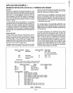
Peripheral Compatibility -
3.125
and 5
MHz
Intel supports its processors with many
LSI
peripheral com-
ponents that do a wide range of functions to simplify circuit
design. The 8085A compatible peripherals have been denoted
the
"-5"
notation to show compatibility. The
"-5"
notation
also signifies that these devices are compatible with the
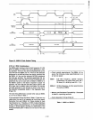
8085A-2 with one wait state interjected. This wait state is
produced by taking the ready line low at the proper time as
shown in Figure
19.
A list of these peripherals is shown
in
Table
6 with corres-
ponding relevant specifications
to
illustrate 8085A-2 compat-
ibility. The
analYSis
for determining the resulting timings is
similar to the analysis
in
the previous memory compatibility
section.
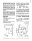
60n,
AS_A15(]
SO,Sl
101M
ROM
etc.
+5V
ALE-----t)
WAIT
100
n'
AVAILABLE
TIME TO
SET-UP
READY
1------10
74S74
Q
tpd -
15n,
tpd - 15ns
CLKOUT-----------~
Figure 19. 8085A·2 Wait State Generator
-lOn,