www.national.com 100
CP3BT26
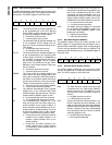
MF The Missed SOF bit is set when the frame
number in a valid received SOF does not
match the expected next value, or when an
SOF is not received within 12060 bit times.
The MF bit provides read-only access. On re-
set, this bit is set. This bit is set by the hard-
ware and is cleared by reading the FNH
register.
0 – No condition indicated.
1 – The frame number in a valid SOF does
not match the expected next value, or no
valid SOF was received within 12060 bit
times.
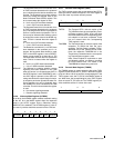
18.3.16 Frame Number Low Byte Register (FNL)
The FNL register holds the low byte of the frame number, as
described above. To ensure consistency, reading this low
byte causes the three frame number bits in the FNH register
to be locked until this register is read. The correct sequence
to read the frame number is: FNL first, followed by FNH.
This register provides read-only access. After reset, the
FNL register is clear.
Note: If the frame counter is updated due to a receipt of a
valid SOF or an artificial update (i.e. missed frame or un-
locked/locked detect), it will take the synchronization ele-
ments a maximum of 2.5 CPU clock cycles to update the
FNH and FNL registers.
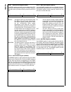
18.3.17 Function Address Register (FAR)
The Function Address Register specifies the device func-
tion address. The different endpoint numbers are set for
each endpoint individually using the Endpoint Control regis-
ters. The FAR register provides read/write access. After re-
set, this register is clear. If the DEF bit in the Endpoint
Control 0 register is set, Endpoint 0 responds to the default
address.
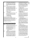
AD The Address field holds the 7-bit function ad-
dress used to transmit and receive all tokens
addressed to this device.
AD_EN The Address Enable bit controls whether the
AD field is used for address comparison. If
not, the device does not respond to any token
on the USB bus.
0 – The device does not respond to any token
on the USB bus.
1 – The AD field is used for address compar-
ison.
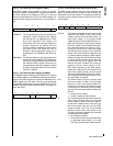
18.3.18 Control Register (DMACNTRL)
The DMACNTRL register controls the main DMA functions
of the CR16 USB node. The DMACTRL register provides
read/write access. This register is clear after reset.
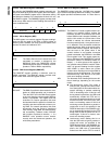
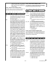
DSRC The DMA Source bit field holds the binary-en-
coded value that specifies which of the end-
points, 1 to 6, is enabled for DMA support. The
DSRC bits are cleared on reset. Table 42
summarizes the DSRC bit settings.
DMOD The DMA Mode bit specifies when a DMA re-
quest is issued. If clear, a DMA request is is-
sued on transfer completion. For transmit
endpoints EP1, EP3, and EP5, the data is
completely transferred, as indicated by the
TX_DONE bit (to fill the FIFO with new trans-
mit data). For receive endpoints EP2, EP4,
and EP6, this is indicated by the RX_LAST bit.
When the DMOD bit is set, a DMA request is
issued when the respective FIFO warning bit
is set. The DMOD bit is cleared after reset.
0 – DMA request is issued on transfer com-
pletion.
1 – DMA request is issued when the respec-
tive FIFO warning bit is set.
ADMA The Automatic DMA bit enables Automatic
DMA (ADMA) and automatically enables the
selected receive or transmit endpoint. Before
ADMA mode can be enabled, the DEN bit in
the DMA Control (DMACNTRL) register must
be cleared. ADMA mode functions until any bit
in the DMA Event (DMAEV) register is set, ex-
cept for NTGL. To initiate ADMA mode, all bits
in the DMAEV register must be cleared, ex-
cept for NTGL.
0 – Automatic DMA disabled.
1 – Automatic DMA enabled.
7 0
FN7:0
7 6 0
AD_EN AD
7 6 5 4 3 2 0
DEN IGNRXTGL DTGL ADMA DMOD DSRC
Table 42 DSRC Bit Description
DSRC Endpoint Number
000 1
001 2
010 3
011 4
100 5
101 6
11x Reserved


