39 www.national.com
CP3BT26
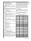
8.5.10 Flash Memory Transition Time Reload
Register (FMTRAN/FSMTRAN)
The FMTRAN/FMSTRAN register is a byte-wide read/write
register that controls some program/erase transition times.
Software must not modify this register while program/erase
operation is in progress (FMBUSY set). At reset, this regis-
ter is initialized to 30h if the flash memory is idle. The CPU
bus master has read/write access to this register.
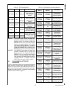
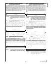
FTTRAN The Flash TIming Transition Count field spec-
ifies a delay of (FTTRAN + 1) prescaler output
clocks.
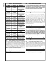
8.5.11 Flash Memory Programming Time Reload
Register (FMPROG/FSMPROG)
The FMPROG/FSMPROG register is a byte-wide read/write
register that controls the programming pulse width. Soft-
ware must not modify this register while a program/erase
operation is in progress (FMBUSY set). At reset, this regis-
ter is initialized to 16h if the flash memory is idle. The CPU
bus master has read/write access to this register.
FTPROG The Flash Timing Programming Pulse Width
field specifies a programming pulse width of
8 × (FTPROG + 1) prescaler output clocks.
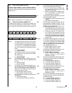
8.5.12 Flash Memory Page Erase Time Reload
Register (FMPERASE/FSMPERASE)
The FMPERASE/FSMPERASE register is a byte-wide
read/write register that controls the page erase pulse width.
Software must not modify this register while a program/
erase operation is in progress (FMBUSY set). At reset, this
register is initialized to 04h if the flash memory is idle. The
CPU bus master has read/write access to this register.
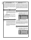
FTPER The Flash Timing Page Erase Pulse Width
field specifies a page erase pulse width of
4096 × (FTPER + 1) prescaler output clocks.
8.5.13 Flash Memory Module Erase Time Reload
Register 0 (FMMERASE0/FSMMERASE0)
The FMMERASE0/FSMMERASE0 register is a byte-wide
read/write register that controls the module erase pulse
width. Software must not modify this register while a pro-
gram/erase operation is in progress (FMBUSY set). At re-
set, this register is initialized to EAh if the flash memory is
idle. The CPU bus master has read/write access to this reg-
ister.
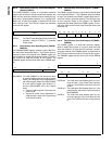
FTMER The Flash Timing Module Erase Pulse Width
field specifies a module erase pulse width of
4096 × (FTMER + 1) prescaler output clocks.
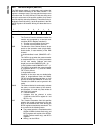
8.5.14 Flash Memory End Time Reload Register
(FMEND/FSMEND)
The FMEND/FSMEND register is a byte-wide read/write
register that controls the delay time after a program/erase
operation. Software must not modify this register while a
program/erase operation is in progress (FMBUSY set). At
reset, this register is initialized to 18h when the flash mem-
ory on the chip is idle. The CPU bus master has read/write
access to this register.
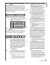
FTEND The Flash Timing End Delay Count field spec-
ifies a delay of (FTEND + 1) prescaler output
clocks.
8.5.15 Flash Memory Module Erase End Time Reload
Register (FMMEND/FSMMEND)
The FMMEND/FSMMEND register is a byte-wide read/write
register that controls the delay time after a module erase op-
eration. Software must not modify this register while a pro-
gram/erase operation is in progress (FMBUSY set). At
reset, this register is initialized to 3Ch if the flash memory is
idle. The CPU bus master has read/write access to this reg-
ister.
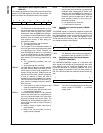
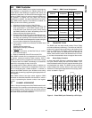
FTMEND The Flash Timing Module Erase End Delay
Count field specifies a delay of 8 × (FTMEND
+ 1) prescaler output clocks.
70
FTTRAN
70
FTPROG
70
FTPER
70
FTMER
70
FTEND
70
FTMEND


