www.national.com 40
CP3BT26
8.5.16 Flash Memory Recovery Time Reload Register
(FMRCV/FSMRCV)
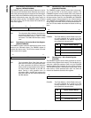
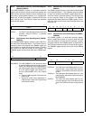
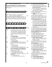
The FMRCV/FSMRCV register is a byte-wide read/write
register that controls the recovery delay time between two
flash memory accesses. Software must not modify this reg-
ister while a program/erase operation is in progress (FM-
BUSY set). At reset, this register is initialized to 04h if the
flash memory is idle. The CPU bus master has read/write
access to this register.
FTRCV The Flash Timing Recovery Delay Count field
specifies a delay of (FTRCV + 1) prescaler
output clocks.
8.5.17 Flash Memory Auto-Read Register 0 (FMAR0/
FSMAR0)
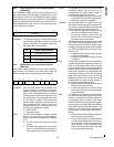
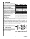
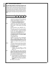
The FMAR0/FSMAR0 register contains a copy of the Func-
tion Word from Information Block 0. The Function Word is
sampled at reset. The contents of the FMAR0 register are
used to enable or disable special device functions. The CPU
bus master has read-only access to this register. The
FSMAR0 register has the same value as the FMAR0 regis-
ter
USB_ENABLE
The USB_ENABLE bit can be used to force
an external USB transceiver into its low-power
mode. The USB power mode is dependent on
the USB controller status, the USB_ENABLE
bit in the MCFG register (see Section 7.1),
and the USB_ENABLE bit in the Function
Word.
0
– External USB transceiver forced into low-
power mode.
1
– Transceiver power mode dependent on
USB controller status and programming
of the Function Word.
8.5.18 Flash Memory Auto-Read Register 1 (FMAR1/
FSMAR1)
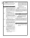
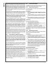
The FMAR1 register contains a copy of the Protection Word
from Information Block 1. The Protection Word is sampled
at reset. The contents of the FMAR1 register define the cur-
rent Flash memory protection settings. The CPU bus mas-
ter has read-only access to this register. The FSMAR1
register has the same value as the FMAR1 register. The for-
mat is the same as the format of the Protection Word (see
Section 8.4.2).
8.5.19 Flash Memory Auto-Read Register 2 (FMAR2/
FSMAR2)
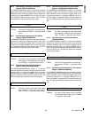
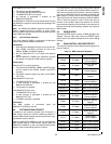
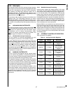
The FMAR2 register is a word-wide read-only register,
which is loaded during reset. It is used to build the Code
Area start address. At reset, the CPU executes a branch,
using the contents of the FMAR2 register as displacement.
The CPU bus master has read-only access to this register.
The FSMAR2 register has the same value as the FMAR2
register.
CADR10:0 The Code Area Start Address (bits 10:0) con-
tains the lower 11 bits of the Code Area start
address. The CADR10:0 field has a fixed val-
ue of 0.
CADR14:11 The Code Area Start Address (bits 14:11) are
loaded during reset with the inverted value of
BOOTAREA3:0.
CADR15 The Code Area Start Address (bits 15) con-
tains the upper bit of the Code Area start ad-
dress. The CADR15 field has a fixed value of
0.
70
FTRCV
15 1 0
Reserved USB_ENABLE
15 13 12 10 9 7 6 4 3 1 0
WRPROT RDPROT ISPE EMPTY BOOTAREA 1
70
CADR7:0
15 14 11 10 8
CADR15
CADR14:11 CADR10:8


