www.national.com 80
CP3BT26
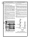
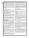
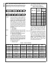
The output of the Input Multiplexer is available externally as
the MUXOUT0 and MUXOUT1 signals. In single-ended
mode, only MUXOUT0 is used. In differential mode,
MUXOUT0 is the positive side and MUXOUT1 is the nega-
tive side. The MUXOUT0 and MUXOUT1 outputs and the
ADCIN external analog input are provided so that external
signal conditioning circuits (such as filters) may be applied
to the analog signals before conversion. The MUXOUT0,
MUXOUT1, and ADCIN signals are alternate functions of
GPIO pins used by the Input Multiplexer, so the number of
available analog input channels is reduced when these sig-
nals are used.
16.1.2 Operation
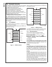
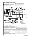
The TRIGGER block may be configured to initiate a conver-
sion from either of these sources:
External ASYNC Input—an edge on the ASYNC input
triggers a conversion. This input may be configured to be
sensitive to rising or falling edges, as controlled by the
POL bit in the ADCCNTRL register.
ADCSTART Register—writing any value to the ADC-
START register triggers a conversion.
The TRIGGER block incorporates a glitch filter to suppress
transient spikes on the ASYNC input. The TRIGGER block
will recognize ASYNC pulse widths of 10 ns or greater.
Once a trigger event has been recognized, no further trig-
gering is recognized until the conversion is completed.
When the ASYNC input is selected as the trigger source, it
may be configured for automatic or non-automatic mode, as
controlled by the AUTO bit in the ADCCNTRL register:
Automatic Mode—a conversion is triggered by any
qualified edge on the ASYNC input (unless a conversion
is already in progress).
Non-Automatic Mode—before a conversion may be
triggered from the ASYNC input, software must “prime”
the TRIGGER block by writing the ADCSTART register.
Once the TRIGGER block is primed, a conversion is trig-
gered by any qualified edge on the ASYNC input. After
the conversion is completed, no additional trigger events
will be recognized until software once again primes the
TRIGGER block by writing the ADCSTART register.
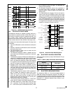
Once a trigger event is recognized, the DELAY1 block waits
for a programmable delay specified in the ADC_DELAY1
field of the ADCSCDLY register. Then, it asserts the Start
signal to the ADC SEQUENCER block.
When the Start signal is received, the ADC SEQUENCER
block initiates the conversion in the 12-Bit ADC. After the
conversion is complete, the result is loaded into the FIFO,
and the Done signal is asserted.
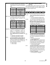
The ADCRESLT register includes the software-visible end
of a 4-word FIFO, which allows up to 4 conversion results to
be queued for reading. Reading the ADCRESLT register un-
loads the FIFO. If the FIFO overflows, a bit is set in the AD-
CRESLT register, and the most recent conversion data is
lost.
The Done signal is visible to software as the ADC_DONE bit
in the ADCRESLT register. The Done signal is also an input
to the interrupt controller (IRQ13). The interrupt will be as-
serted whenever the FIFO is not empty (but will deassert for
one system clock after the ADCRESLT register is read). To-
tal conversion time is around 15 microseconds.
The Done signal is also an input to the Multi-Input Wake-Up
unit (WUI30). The MIWU input is asserted whenever the
FIFO is not empty (but will deassert for one system clock af-
ter the ADCRESLT register is read). The wake-up output is
provided so that the ADC module can bring the system out
of a power-saving mode when a conversion operation is
completed. It asserts earlier than the interrupt output. In the
pen-down detection mode of the ADC, the wake-up output
is ORed with the ADC pen-down detector output, to wake up
on a pen-down event.
16.1.3 ADC Clock Generation
The DELAY2 block generates ADC Clock, which is the clock
used internally by the ADC module. ADC Clock is derived
from either:
System Clock—a programmable divider is available to
generate the 12 MHz clock required by the ADC from the
System Clock.
Auxiliary Clock 2—may be used to perform conversions
when the System Clock is slowed down or suspended in
low-power modes.
The DELAY2 block receives the clock source selected by
the CLKSEL bit of the ADCACR register and adds a number
of asynchronous incremental delay units specified in the
ADC_DELAY2 field of the ADCSCDLY register. This de-
layed clock (ADC Clock) then drives the TRIGGER, 12-BIT
ADC, and ADC SEQUENCER blocks. ADC Clock also
drives the ADC_DIV clock divider, which generates the
clock which drives the DELAY1 block.
Because the ADCRESLT FIFO is driven by System Clock
(not ADC Clock), a conversion result will not propagate to
the output of the FIFO when the System Clock is suspend-
ed.
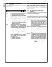
16.1.4 ADC Voltage References
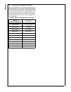
The 12-BIT ADC block has positive and negative voltage
reference inputs, VREFP and VREFN. In single-ended
mode, only VREFP is used. An analog multiplexer allows
selecting an external VREFP pin, the analog supply voltage
AVCC, or the analog inputs ADC0 or ADC1 as the positive
voltage reference, as controlled by the PREF_CFG field of
the ADCGCR register. Another analog multiplexer allows
selecting the analog ground AGND or the analog inputs
ADC2 or ADC3 as the negative voltage reference, as con-
trolled by the NREF_CFG field of the ADCGCR register.
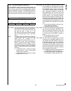
16.1.5 Pen-Down Detector
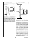
A pen-down detector is provided on the ADC0 (TSX+) input
of the ADC. It consists of a Schmitt-trigger receiver, with a
minimum Vil of 0.7V. When pen-down detect mode is en-
abled by loading 101b into the TOUCH_CFG field of the AD-
CGCR register, the output of this detector is visible to
software in the PEN_DOWN bit of the ADCRESLT register,
and this output is ORed with the Done signal to become the
wake-up input (WUI30) to the Multi-Input Wake-Up unit.


