www.national.com 170
CP3BT26
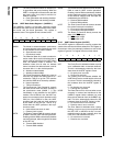
UPEN The Parity Enable bit enables or disables par-
ity generation and parity checking. When the
UART is configured to transmit nine data bits
per frame, there is no parity bit and the Un-
PEN bit is ignored.
0 – Parity generation and checking disabled.
1 – Parity generation and checking enabled.
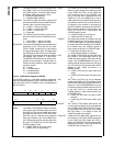
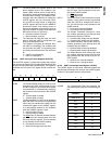
22.3.6 UART Mode Select Register 1 (UnMDSL1)
The UnMDSL1 register is a byte-wide, read/write register
that selects the clock source, synchronization mode, atten-
tion mode, and line break generation. This register is
cleared at reset. The register format is shown below.
UMOD The Mode bit selects between synchronous
and asynchronous mode. Synchronous mode
is only available for the UART0 module.
0 – Asynchronous mode.
1 – Synchronous mode.
UATN The Attention Mode bit is used to enable At-
tention mode. When set, this bit selects the at-
tention mode of operation for the UART. When
clear, the attention mode is disabled. The
hardware clears this bit after an address
frame is received. An address frame is a 9-bit
character with a 1 in the ninth bit position.
0 – Attention mode disabled.
1 – Attention mode enabled.
UBRK The Force Transmission Break bit is used to
force the TXD output low. Setting this bit to 1
causes the TXD pin to go low. TXD remains
low until the UBRK bit is cleared by software.
0 – Normal operation.
1 – TXD pin forced low.
UCKS The Synchronous Clock Source bit controls
the clock source when the UART operates in
the synchronous mode (UMOD = 1). This
functionality is only available for the UART0
module. If the UCKS bit is set, the UART op-
erates from an external clock provided on the
CKX pin. If the UCKS bit is clear, the UART
operates from the baud rate clock produced
by the UART on the CKX pin. This bit is ig-
nored when the UART operates in the asyn-
chronous mode.
0 – Internal baud rate clock is used.
1 – External clock is used.
UETD The Enable Transmit DMA bit controls wheth-
er DMA is used for UART transmit operations.
Enabling transmit DMA automatically disables
transmit interrupts, without regard to the state
of the UETI bit.
0 – Transmit DMA disabled.
1 – Transmit DMA enabled.
UERD The Enable Receive DMA bit controls whether
DMA is used for UART receive operations.
Enabling receive DMA automatically disables
receive interrupts, without regard to the state
of the UERI bit. Receive error interrupts are
unaffected by the UERD bit.
0 – Receive DMA disabled.
1 – Receive DMA enabled.
UFCE The Flow Control Enable bit controls whether
flow control interrupts are enabled.
0 – Flow control interrupts disabled.
1 – Flow control interrupts enabled.
URTS The Ready To Send bit directly controls the
state of the RTS
output.
0 – RTS
output is high.
1 – RTS output is low.
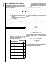
22.3.7 UART Status Register (UnSTAT)
The UnSTAT register is a byte-wide, read-only register that
contains the receive and transmit status bits. This register is
cleared upon reset. Any attempt by software to write to this
register is ignored. The register format is shown below.
UPE The Parity Error bit indicates whether a parity
error is detected within a received character.
This bit is automatically cleared by the hard-
ware when the UnSTAT register is read.
0 – No parity error occurred.
1 – Parity error occurred.
UFE The Framing Error bit indicates whether the
UART fails to receive a valid stop bit at the end
of a frame. This bit is automatically cleared by
the hardware when the UnSTAT register is
read.
0 – No framing error occurred.
1 – Framing error occurred.
UDOE The Data Overrun Error bit is set when a new
character is received and transferred to the
UnRBUF register before software has read
the previous character from the UnRBUF reg-
ister. This bit is automatically cleared by the
hardware when the UnSTAT register is read.
0 – No receive overrun error occurred.
1 – Receive overrun error occurred.
UERR The Error Status bit indicates when a parity,
framing, or overrun error occurs (any time that
the UPE, UFE, or UDOE bit is set). It is auto-
matically cleared by the hardware when the
UPE, UFE, and UDOE bits are all 0.
0 – No receive error occurred.
1 – Receive error occurred.
7 6 5 4 3 2 1 0
URTS UFCE UERD
UETD UCKS UBRK
UATN
UMOD
7 6 5 4 3 2 1 0
Res.
UXMIP
URB9 UBKD UERR UDOE UFE UPE


