www.national.com 26
CP3BT26
6.4.2 I/O Zone Configuration Register (IOCFG)
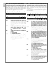
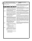
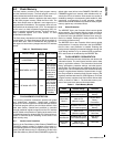
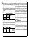
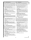
The IOCFG register is a word-wide, read/write register that
controls the timing and bus characteristics of accesses to
the 256-byte I/O Zone memory space (FF FB00h to FF
FBFFh). The registers associated with Port B and Port C re-
side in the I/O memory array. At reset, the register is initial-
ized to 069Fh. The register format is shown below.
WAIT The Memory Wait Cycles field specifies the
number of TIW (internal wait state) clock cy-
cles added for each memory access, ranging
from 000 binary for no additional TIW wait cy-
cles to 111 binary for seven additional TIW
wait cycles.
HOLD The Memory Hold Cycles field specifies the
number of T
hold
clock cycles used for each
memory access, ranging from 00b for no
T
hold
cycles to 11b for three T
hold
clock cy-
cles.
BW The Bus Width bit defines the bus width of the
IO Zone.
0
– 8-bit bus width.
1 – 16-bit bus width (default)
IPST The Post Idle bit controls whether an idle cycle
follows the current bus cycle, when the next
bus cycle accesses a different zone. No idle
cycles are required for on-chip accesses.
0
– No idle cycle (recommended).
1 – Idle cycle.
6.4.3 Static Zone 0 Configuration Register (SZCFG0)
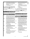
The SZCFG0 register is a word-wide, read/write register
that controls the timing and bus characteristics of Zone 0
memory accesses. Zone 0 is used for the on-chip flash
memory (including the boot area, program memory, and
data memory).
At reset, the register is initialized to 069Fh. The register for-
mat is shown below.
WAIT The Memory Wait field specifies the number
of TIW (internal wait state) clock cycles added
for each memory access, ranging from 000b
for no additional TIW wait cycles to 111b for
seven additional TIW wait cycles. These bits
are ignored if the SZCFG0.FRE bit is set.
HOLD The Memory Hold field specifies the number
of T
hold
clock cycles used for each memory
access, ranging from 00b for no T
hold
cycles
to 11b for three T
hold
clock cycles. These bits
are ignored if the SZCFG0.FRE bit is set.
RBE The Read Burst Enable enables burst cycles
on 16-bit reads from 8-bit bus width regions of
the address space. Because the flash pro-
gram memory is required to be 16-bit bus
width, the RBE bit is a don’t care bit. This bit
is ignored when the SZCFG0.FRE bit is set.
0
– Burst read disabled.
1 – Burst read enabled.
WBR The Wait on Burst Read bit controls if a wait
state is added on burst read transaction. This
bit is ignored, when SZCFG0.FRE bit is set or
when SZCFG0.RBE is clear.
0
– No TBW on burst read cycles.
1 – One TBW on burst read cycles.
BW The Bus Width bit controls the bus width of the
zone. The flash program memory must be
configured for 16-bit bus width.
0
– 8-bit bus width.
1
– 16-bit bus width (required).
FRE The Fast Read Enable bit controls whether
fast read bus cycles are used. A fast read op-
eration takes one clock cycle. A normal read
operation takes at least two clock cycles.
0
– Normal read cycles.
1
– Fast read cycles.
IPST The Post Idle bit controls whether an idle cycle
follows the current bus cycle, when the next
bus cycle accesses a different zone. No idle
cycles are required for on-chip accesses.
0
– No idle cycle (recommended).
1
– Idle cycle inserted.
7 6 5 4 3 2 0
BW Reserved HOLD WAIT
15 10 9 8
Reserved IPST Res.
7 6 5 4 3 2 0
BW WBR RBE HOLD WAIT
15 12 11 10 9 8
Reserved FRE IPRE IPST Res.


