37 www.national.com
CP3BT26
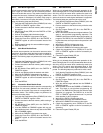
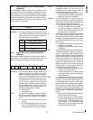
8.5.5 Flash Data Memory 0 Write Enable Register
(FSM0WER)
The FSM0WER register controls write protection for the
flash data memory. The data block is divided into 16 512-
byte sections. Each bit in the FSM0WER register controls
write protection for one of these sections. The FSM0WER
register is cleared after device reset, so the flash memory is
write protected after reset. The CPU bus master has read/
write access to this registers.
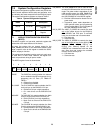
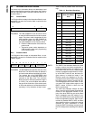
FSM0WEn The Flash Data Memory 0 Write Enable n bits
control write protection for a section of a flash
memory data block. The address mapping of
the register bits is shown below.
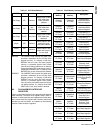
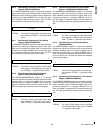
8.5.6 Flash Memory Control Register (FMCTRL/
FSMCTRL)
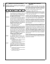
This register controls the basic functions of the Flash pro-
gram memory. The register is clear after device reset. The
CPU bus master has read/write access to this register.
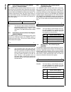
LOWPRW The Low Power Mode controls whether flash
program memory is operated in low-power
mode, which draws less current when data is
read. This is accomplished be only accessing
the flash program memory during the first half
of the clock period. The low-power mode must
not be used at System Clock frequencies
above 25 MHz, otherwise a read access may
return undefined data. This bit must not be
changed while the flash program memory is
busy being programmed or erased.
0
– Normal mode.
1
– Low-power mode.
CWD The CPU Write Disable bit controls whether
the CPU has write access to flash memory.
This bit must not be changed while FMBUSY
is set.
0
– The CPU has write access to the flash
memory
1 – An external debugging tool is the current
“owner” of the flash memory interface, so
write accesses by the CPU are inhibited.
DISVRF The Disable Verify bit controls the automatic
verification feature. This bit must not be
changed while the flash program memory is
busy being programmed or erased.
0
– New flash program memory contents are
automatically verified after programming.
1
– Automatic verification is disabled.
IENPROG The Interrupt Enable for Program bit is clear
after reset. The flash program and data mem-
ories share a single interrupt channel but have
independent interrupt enable control bits.
0
– No interrupt request is asserted to the
ICU when the FMFULL bit is cleared.
1 – An interrupt request is made when the
FMFULL bit is cleared and new data can
be written into the write buffer.
PE The Program Enable bit controls write access
of the CPU to the flash program memory. This
bit must not be altered while the flash program
memory is busy being programmed or erased.
The PER and MER bits must be clear when
this bit is set.
0
– Programming the flash program memory
by the CPU is disabled.
1
– Programming the flash program memory
is enabled.
PER The Page Erase Enable bit controls whether a
a valid write operation triggers an erase oper-
ation on a 1024-byte page of flash memory.
Page erase operations are only supported for
the main blocks, not the information blocks. A
page erase operation on an information block
is ignored and does not alter the information
block. When the PER bit is set, the PE and
MER bits must be clear. This bit must not be
changed while the flash program memory is
busy being programmed or erased.
0
– Page erase mode disabled. Write opera-
tions are performed normally.
1
– A valid write operation to a word location
in program memory erases the page that
contains the word.
MER The Module Erase Enable bit controls wheth-
er a valid write operation triggers an erase op-
eration on an entire block of flash memory. If
an information block is written in this mode,
both the information block and its correspond-
ing main block are erased. When the MER bit
is set, the PE and PER bits must be clear. This
bit must not be changed while the flash pro-
gram memory is busy being programmed or
erased.
0
– Module erase mode disabled. Write oper-
ations are performed normally.
1
– A valid write operation to a word location
in a main block erases the block that con-
tains the word. A valid write operation to a
word location in an information block
erases the block that contains the word
and its associated main block.
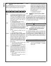
15 0
FSM0WE
Bit Logical Address Range
0 0E 0000h
–0E 01FFh
1–14 . . .
15 0E 1E00h–0E 1FFFh
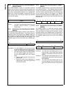
7 6 5 4 3 2 1 0
MER PER PE IENPROG DISVRF Res. CWD LOWPRW


