www.national.com 246
CP3BT26
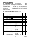
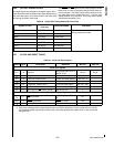
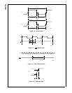
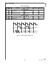
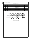
30.5 FLASH MEMORY ON-CHIP PROGRAMMING
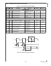
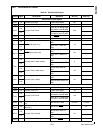
Symbol Parameter Conditions Min Max Units
t
START
Program/Erase to NVSTR Setup Time
a
(NVSTR = Non-Volatile Storage
a. Program/erase to NVSTR Setup Time is determined by the following equation:
t
START
= T
clk
× (FTDIV + 1) × (FTSTART + 1), where T
clk
is the System Clock period, FTDIV is the contents of
the FMPSR or FSMPSR register, and FTSTART is the contents of the FMSTART or FSMSTART register
5-µs
t
TRAN
NVSTR to Program Setup Time
b
b. NVSTR to Program Setup Time is determined by the following equation:
t
TRAN
= T
clk
× (FTDIV + 1) × (FTTRAN + 1), where T
clk
is the System Clock period, FTDIV is the contents of
the FMPSR or FSMPSR register, and FTTRAN is the contents of the FMTRAN or FSMTRAN register
10 - µs
t
PROG
Programming Pulse Width
c
c. Programming Pulse Width is determined by the following equation:
t
PROG
= T
clk
× (FTDIV + 1) × 8 × (FTPROG + 1), where T
clk
is the System Clock period, FTDIV is the con-
tents of the FMPSR or FSMPSR register, and FTPROG is the contents of the FMPROG or FSMPROG regis-
ter
20 40 µs
t
PERASE
Page Erase Pulse Width
d
d. Page Erase Pulse Width is determined by the following equation:
t
PERASE
= T
clk
× (FTDIV + 1) × 4096 × (FTPER + 1), where T
clk
is the System Clock period, FTDIV is the
contents of the FMPSR or FSMPSR register, and FTPER is the contents of the FMPERASE or FSMPER-
ASE register
20 - ms
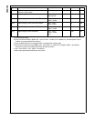
t
MERASE
Module Erase Pulse Width
e
e. Module Erase Pulse Width is determined by the following equation:
t
MERASE
= T
clk
× (FTDIV + 1) × 4096 × (FTMER + 1), where T
clk
is the System Clock period, FTDIV is the
contents of the FMPSR or FSMPSR register, and FTMER is the contents of the FMMERASE0 or
FSMMERASE0 register
200 - ms
t
END
NVSTR Hold Time
f
f. NVSTR Hold Time is determined by the following equation:
t
END
= T
clk
× (FTDIV + 1) × (FTEND + 1), where T
clk
is the System Clock period, FTDIV is the contents of the
FMPSR or FSMPSR register, and FTEND is the contents of the FMEND or FSMEND register
5-µs
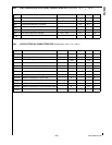
t
MEND
NVSTR Hold Time (Module Erase)
g
g. NVSTR Hold Time (Module Erase) is determined by the following equation:
t
MEND
= T
clk
× (FTDIV + 1) × 8 × (FTMEND + 1), where T
clk
is the System Clock period, FTDIV is the con-
tents of the FMPSR or FSMPSR register, and FTMEND is the contents of the FMMEND or FSMMEND regis-
ter
100 - µs
t
RCV
Recovery Time
h
h. Recovery Time is determined by the following equation:
t
RCV
= T
clk
× (FTDIV + 1) × (FTRCV + 1), where T
clk
is the System Clock period, FTDIV is the contents of the
FMPSR or FSMPSR register, and FTRCV is the contents of the FMRCV or FSMRCV register
1-µs
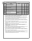
t
HV
Cumulative Program High Voltage Period For
Each Row After Erase
i
i. Cumulative program high voltage period for each row after erase t
HV
is the accumulated duration a flash cell
is exposed to the programming voltage after the last erase cycle.
128K program blocks - 8 ms
t
HV
8K data block - 4 ms
Write/Erase Endurance 20,000 - cycles
Data Retention 25°C100-years


