www.national.com 84
CP3BT26
16.5.1 ADC Global Configuration Register (ADCGCR)
The ADCGCR register controls the basic operation of the in-
terface. The CPU bus master has read/write access to the
ADCGCR register. After reset this register is set to 0000h.
CLKEN The Clock Enable bit controls whether the
ADC module is running. When this bit is clear,
all ADC clocks are disabled, the ADC analog
circuits are in a low-power state, and ADC
registers (other than the ADCGCR and AG-
CACR registers) are not writeable. Clearing
this bit reinitializes the ADC state machine
and cancels any pending trigger event. When
this bit is set, the ADC clocks are enabled and
the ADC analog circuits are powered up. The
converter is operational within 0.25 µs of be-
ing enabled.
0 – ADC disabled.
1 – ADC enabled.
ADCIN The ADCIN bit selects the source of the ADC
input. When the bit is clear, the source is the
8-channel Input Multiplexer. When the bit is
set, the source is the ADCIN pin.
0 – ADC input is from 8-channel multiplexer.
1 – ADC input is from ADCIN pin.
DIFF The Differential Operation Mode bit and the
MUX_CFG field configure the analog circuits
of the ADC module. When this bit is clear, the
ADC module operates in single-ended mode.
When this bit is set, the ADC operates in dif-
ferential mode. See Table 35 .
0 – Single-ended mode.
1 – Differential mode.
MUX_CFG The Multiplexer Configuration field and the
DIFF bit configure the analog circuits of the
ADC module, as shown in Table 35.
For best noise immunity in touchscreen appli-
cations, channel 2 should be used for sam-
pling the X plate voltage, and channel 1
should be used for sampling the Y plate volt-
age.
TOUCH_CFG
The Touchscreen Configuration field controls
the configuration of the low-ohmic drivers for
the TSX+, TSX-, TSY+, and TSY- signals, as
shown in Table 36. When TOUCH_CFG is
101b, the pen-down detector is enabled. The
output of the pen-down detector is visible to
software in the PEN_DOWN bit of the AD-
SRESLT register, and it is ORed with the
Done signal to generate the wake-up signal
WUI30 passed to the MIWU unit.
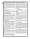
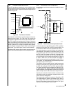
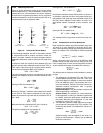
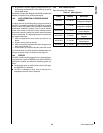
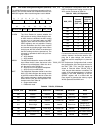
8765432 1 0
TOUCH_CFG MUX_CFG DIFF ADCIN CLKEN
15 14 13 12 11 10 9
MUXOUTEN INTEN Res. NREF_CFG PREF_CFG
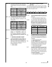
Table 35 MUX_CFG Operation
MUX_CFG
Channel
Selected,
(DIFF = 0)
Channels
Selected
(DIFF = 1)
+-
000 0 0 1
001 1 1 0
010 2 2 3
011 3 3 2
100 4 4 5
101 5 5 4
110 6 6 7
111 7 7 6
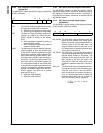
Table 36 TOUCH_CFG Modes
TOUCH_CFG ADC0/TSX+ ADC1/TSY+ ADC2/TSX- ADC3/TSY- Mode
000 Inactive Inactive Inactive Inactive None
001 Inactive Driven High Inactive Driven Low Sample Y
010 Driven High Inactive Driven Low Inactive Sample X
011 Driven High Inactive Inactive Driven Low
Sample Z (1),
Pre-Pen Down
100 Inactive Driven High Driven Low Inactive Sample Z (2)
101 Weakly Pulled High Inactive Inactive Driven Low Pen-Down Detect
11X Inactive Inactive Inactive inactive Reserved


