www.national.com 32
CP3BT26
8.2.1 Main Block 0 and 1
Main Block 0 and Main Block 1 hold the 256K-byte program
space, which consists of the Boot Area and Code Area.
Each block consists of sixteen 8K-byte sections. Write ac-
cess by the CPU to Main Block 0 and Main Block 1 is con-
trolled by the corresponding bits in the FM0WER and
FM1WER registers, respectively. The least significant bit in
each register controls the section at the lowest address.
8.2.2 Information Block 0
Information Block 0 contains 128 bytes, of which one 16-bit
word has a dedicated function, called the Function Word.
The Function Word resides at address 07Eh. It controls the
power mode of an external USB transceiver. The remaining
Information Block 0 locations are used to hold factory pa-
rameters.
Software only has read access to Information Block 0
through a register-based interface. The Function Word and
the factory parameters are protected against CPU writes.
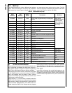
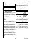
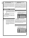
Table 12 shows the structure of Information Block 0.
Table 12 Information Block 0
8.2.3 Information Block 1
Information Block 1 contains 128 bytes, of which one 16-bit
word has a dedicated function, called the Protection Word.
The Protection Word resides at address 0FEh. It controls
the global protection mechanisms and the size of the Boot
Area. The Protection Word can be written by the CPU, how-
ever the changes only become valid after the next device re-
set. The remaining Information Block 1 locations can be
used to store other user data. Erasing Information Block 1
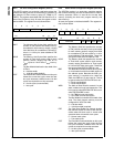
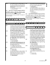
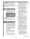
also erases Main Block 1. Table 13 shows the structure of
the Information Block 1.
Table 13 Information Block 1
8.2.4 Main Block 2
Main Block 2 holds the 8K-byte data area, which consists of
sixteen 512-byte sections. Write access by the CPU to Main
Block 2 is controlled by the corresponding bits in the
FSM0WER register. The least significant bit in the register
controls the section at the lowest address.
8.2.5 Information Block 2
Information Block 2 contains 128 bytes, which can be used
to store user data. The CPU can always read Information
Block 2. The CPU can write Information Block 2 only when
global write protection is disabled. Erasing Information
Block 2 also erases Main Block 2.
8.3 FLASH MEMORY OPERATIONS
Flash memory programming (erasing and writing) can be
performed on the flash data memory while the CPU is exe-
cuting out of flash program memory. Although the CPU can
execute out of flash data memory, it cannot erase or write
the flash program memory while executing from flash data
memory. To erase or write the flash program memory, the
CPU must be executing from the on-chip static RAM or off-
chip memory.
An erase operation is required before programming. An
erase operation sets all of the bits in the erased region. A
programming operation clears selected bits.
The programming mechanism is pipelined, so that a new
write request can be loaded while a previous request is in
progress. When the FMFULL bit in the FMSTAT or FSM-
STAT register is clear, the pipeline is ready to receive a new
request. New requests may be loaded after checking only
the FMFULL bit.
8.3.1 Main Block Read
Read accesses from flash program memory can only occur
when the flash program memory is not busy from a previous
write or erase operation. Read accesses from the flash data
memory can only occur when both the flash program mem-
ory and the flash data memory are not busy. Both byte and
word read operations are supported.
8.3.2 Information Block Read
Information block data is read through the register-based in-
terface. Only word read operations are supported and the
read address must be word-aligned (LSB = 0). The following
steps are used to read from an information block:
1. Load the word address in the Flash Memory Informa-
tion Block Address (FMIBAR) or Flash Slave Memory
Information Block Address (FSMIBAR) register.
2. Read the data word by reading out the Flash Memory
Information Block Data (FMIBDR) or Flash Slave Mem-
ory Information Block Data (FSMIBDR) register.
Name
Address
Range
Read
Access
Write Access
Function
Word
07Eh
–07Fh
Ye s N o
Other (Used
for Factory
Parameters)
000h
–07Dh
Name
Address
Range
Read
Access
Write Access
Protection
Word
0FEh
–0FFh
Ye s
Write access only
if section write
enable bit is set
and global write
protection is dis-
abled.
Other
(User Data)
080h
–0FDh


