www.national.com 4
CP3BT26
3.0 Device Overview
The CP3BT26 connectivity processor is a complete micro-
computer with all system timing, interrupt logic, program
memory, data memory, and I/O ports included on-chip, mak-
ing it well-suited to a wide range of embedded applications.
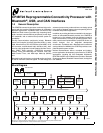
The block diagram on page 1 shows the major on-chip com-
ponents of the CP3BT26 devices.
3.1 CR16C CPU CORE
The CP3BT26 device implements the CR16C CPU core
module. The high performance of the CPU core results from
the implementation of a pipelined architecture with a two-
bytes-per-cycle pipelined system bus. As a result, the CPU
can support a peak execution rate of one instruction per
clock cycle.
For more information, please refer to the CR16C Program-
mer’s Reference Manual (document number 424521772-
101, which may be downloaded from National’s web site at
http://www.national.com).
3.2 MEMORY
The CP3BT26 devices support a uniform linear address
space of up to 16 megabytes. Three types of on-chip mem-
ory occupy specific regions within this address space, along
with any external memory:
256K bytes of Flash program memory
8K bytes of Flash data memory
32K bytes of static RAM
Up to 12M bytes of external memory (144-pin devices)
The 256K bytes of Flash program memory are used to store
the application program, Bluetooth protocol stack, and real-
time operating system. The Flash memory has security fea-
tures to prevent unintentional programming and to prevent
unauthorized access to the program code. This memory
can be programmed with an external programming unit or
with the device installed in the application system (in-sys-
tem programming).
The 8K bytes of Flash data memory are used for non-vola-
tile storage of data entered by the end-user, such as config-
uration settings.
The 32K bytes of static RAM are used for temporary storage
of data and for the program stack and interrupt stack. Read
and write operations can be byte-wide or word-wide, de-
pending on the instruction executed by the CPU.
Up to 12M bytes of external memory can be added on an
external bus. The external bus is only available on devices
in 144-pin packages.
For Flash program and data memory, the device internally
generates the necessary voltages for programming. No ad-
ditional power supply is required.
3.3 INPUT/OUTPUT PORTS
The device has up to 54 software-configurable I/O pins, or-
ganized into seven ports called Port B, Port C, Port E, Port
G, Port H, Port I, and Port J. Each pin can be configured to
operate as a general-purpose input or general-purpose out-
put. In addition, many I/O pins can be configured to operate
as inputs or outputs for on-chip peripheral modules such as
the UART, timers, or Microwire/SPI interface.
The I/O pin characteristics are fully programmable. Each pin
can be configured to operate as a TRI-STATE output, push-
pull output, weak pull-up input, or high-impedance input.
3.4 BUS INTERFACE UNIT
The Bus Interface Unit (BIU) controls access to internal/ex-
ternal memory and I/O. It determines the configured param-
eters for bus access (such as the number of wait states for
memory access) and issues the appropriate bus signals for
each requested access.
The BIU uses a set of control registers to determine how
many wait states and hold states are used when accessing
Flash program memory and the I/O area. At start-up, the
configuration registers are set for slowest possible memory
access. To achieve fastest possible program execution, ap-
propriate values must be programmed. These settings vary
with the clock frequency and the type of off-chip device be-
ing accessed.
3.5 INTERRUPT CONTROL UNIT (ICU)
The ICU receives interrupt requests from internal and exter-
nal sources and generates interrupts to the CPU. An inter-
rupt is an event that temporarily stops the normal flow of
program execution and causes a separate interrupt handler
to be executed. After the interrupt is serviced, CPU execu-
tion continues with the next instruction in the program fol-
lowing the point of interruption.
Interrupts from the timers, UARTs, Microwire/SPI interface,
and Multi-Input Wake-Up, are all maskable interrupts; they
can be enabled or disabled by software. There are 47
maskable interrupts, assigned to 47 linear priority levels.
The highest-priority interrupt is the Non-Maskable Interrupt
(NMI
), which is generated by a signal received on the NMI
input pin.
3.6 MULTI-INPUT WAKE-UP
The two Multi-Input Wake-Up (MIWU) modules can be used
for two purposes: to provide inputs for waking up (exiting)
from the Halt, Idle, or Power Save mode, and to provide gen-
eral-purpose edge-triggered maskable interrupts to the lev-
el-sensitive interrupt control unit (ICU) inputs. Each 16-
channel module generates four programmable interrupts to
the ICU, for a total of 8 ICU inputs generated from 32 MIWU
inputs. Channels can be individually enabled or disabled,
and programmed to respond to positive or negative edges.


