163 www.national.com
CP3BT26
22.0 UART Modules
The CP3BT26 provides four UART modules. Each UART
module is a full-duplex Universal Asynchronous Receiver/
Transmitter that supports a wide range of software-pro-
grammable baud rates and data formats. It handles auto-
matic parity generation and several error detection
schemes.
All UART modules offer the following features:
Full-duplex double-buffered receiver/transmitter
Asynchronous operation
Programmable baud rate
Programmable framing formats: 7, 8, or 9 data bits; even,
odd, or no parity; one or two stop bits (mark or space)
Hardware parity generation for data transmission and
parity check for data reception
Interrupts on “transmit ready” and “receive ready” condi-
tions, separately enabled
Software-controlled break transmission and detection
Internal diagnostic capability
Automatic detection of parity, framing, and overrun errors
One module, UART0, offers the following additional fea-
tures:
Synchronous operation using the CKX external clock pin
Hardware flow control (CTS
and RTS signals)
DMA capability
22.1 FUNCTIONAL OVERVIEW
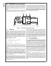
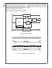
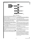
Figure 76 is a block diagram of the UART module showing
the basic functional units in the UART:
Transmitter
Receiver
Baud Rate Generator
Control and Error Detection
The Transmitter block consists of an 8-bit transmit shift reg-
ister and an 8-bit transmit buffer. Data bytes are loaded in
parallel from the buffer into the shift register and then shifted
out serially on the TXD pin.
The Receiver block consists of an 8-bit receive shift register
and an 8-bit receive buffer. Data is received serially on the
RXD pin and shifted into the shift register. Once eight bits
have been received, the contents of the shift register are
transferred in parallel to the receive buffer.
The Transmitter and Receiver blocks both contain exten-
sions for 9-bit data transfers, as required by the 9-bit and
loopback operating modes.
The Baud Rate Generator generates the clock for the syn-
chronous and asynchronous operating modes. It consists of
two registers and a two-stage counter. The registers are
used to specify a prescaler value and a baud rate divisor.
The first stage of the counter divides the UART clock based
on the value of the programmed prescaler to create a slower
clock. The second stage of the counter creates the baud
rate clock by dividing the output of the first stage based on
the programmed baud rate divisor.
The Control and Error Detection block contains the UART
control registers, control logic, error detection circuit, parity
generator/checker, and interrupt generation logic. The con-
trol registers and control logic determine the data format,
mode of operation, clock source, and type of parity used.
The error detection circuit generates parity bits and checks
for parity, framing, and overrun errors.
The Flow Control Logic block provides the capability for
hardware handshaking between the UART and a peripheral
device. When the peripheral device needs to stop the flow
of data from the UART, it de-asserts the clear-to-send (CTS
)
signal which causes the UART to pause after sending the
current frame (if any). The UART asserts the ready-to-send
(RTS
) signal to the peripheral when it is ready to send a
character.
22.2 UART OPERATION
The UART has two basic modes of operation: synchronous
and asynchronous. Synchronous mode is only supported
for the UART0 module. In addition, there are two special-
purpose modes, called attention and diagnostic. This sec-
tion describes the operating modes of the UART.
22.2.1 Asynchronous Mode
The asynchronous mode of the UART enables the device to
communicate with other devices using just two communica-
tion signals: transmit and receive.
In asynchronous mode, the transmit shift register (TSFT)
and the transmit buffer (UnTBUF) double-buffer the data for
transmission. To transmit a character, a data byte is loaded
in the UnTBUF register. The data is then transferred to the
TSFT register. While the TSFT register is shifting out the
current character (LSB first) on the TXD pin, the UnTBUF
register is loaded by software with the next byte to be trans-
mitted. When TSFT finishes transmission of the last stop bit
of the current frame, the contents of UnTBUF are trans-
ferred to the TSFT register and the Transmit Buffer Empty
bit (UTBE) is set. The UTBE bit is automatically cleared by
the UART when software loads a new character into the
UnTBUF register. During transmission, the UXMIP bit is set
high by the UART. This bit is reset only after the UART has
sent the last stop bit of the current character and the UnT-
BUF register is empty. The UnTBUF register is a read/write
register. The TSFT register is not software accessible.
In asynchronous mode, the input frequency to the UART is
16 times the baud rate. In other words, there are 16 clock
cycles per bit time. In asynchronous mode, the baud rate
generator is always the UART clock source.
The receive shift register (RSFT) and the receive buffer (Un-
RBUF) double buffer the data being received. The UART re-
ceiver continuously monitors the signal on the RXD pin for a
low level to detect the beginning of a start bit. On sensing
this low level, the UART waits for seven input clock cycles
and samples again three times. If all three samples still in-
dicate a valid low, then the receiver considers this to be a
valid start bit, and the remaining bits in the character frame
are each sampled three times, around the mid-bit position.
For any bit following the start bit, the logic value is found by
majority voting, i.e. the two samples with the same value de-
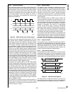
fine the value of the data bit. Figure 77 illustrates the pro-
cess of start bit detection and bit sampling.


