www.national.com 36
CP3BT26
8.5.1 Flash Memory Information Block Address
Register (FMIBAR/FSMIBAR)
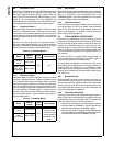
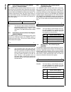
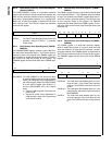
The FMIBAR register specifies the 8-bit address for read or
write access to an information block. Because only word ac-
cess to the information blocks is supported, the least signif-
icant bit (LSB) of the FMIBAR must be 0 (word-aligned). The
hardware automatically clears the LSB, without regard to
the value written to the bit. The FMIBAR register is cleared
after device reset. The CPU bus master has read/write ac-
cess to this register.
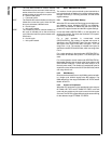
IBA The Information Block Address field holds the
word-aligned address of an information block
location accessed during a read or write
transaction. The LSB of the IBA field is always
clear.
8.5.2 Flash Memory Information Block Data Register
(FMIBDR/FSMIBDR)
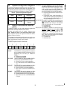
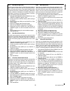
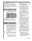
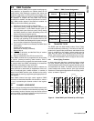
The FMIBDR register holds the 16-bit data for read or write
access to an information block. The FMIBDR register is
cleared after device reset. The CPU bus master has read/
write access to this register.
IBD The Information Block Data field holds the
data word for access to an information block.
For write operations the IBD field holds the
data word to be programmed into the informa-
tion block location specified by the IBA ad-
dress. During a read operation from an
information block, the IBD field receives the
data word read from the location specified by
the IBA address.
8.5.3 Flash Memory 0 Write Enable Register
(FM0WER/FSM0WER)
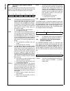
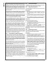
The FM0WER register controls section-level write protec-
tion for the first half of the flash program memory. The
FMS0WER registers controls section-level write protection
for the flash data memory. Each data block is divided into 16
8K-byte sections. Each bit in the FM0WER and FSM0WER
registers controls write protection for one of these sections.
The FM0WER and FSM0WER registers are cleared after
device reset, so the flash memory is write protected after re-
set. The CPU bus master has read/write access to this reg-
isters.
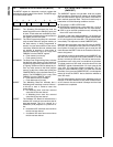
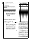
FM0WEn The Flash Memory 0 Write Enable n bits con-
trol write protection for a section of a flash
memory data block. The address mapping of
the register bits is shown below.
8.5.4 Flash Memory 1 Write Enable Register
(FM1WER)
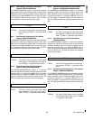
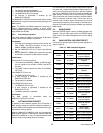
The FM1WER register controls write protection for the sec-
ond half of the program flash memory. The data block is di-
vided into 16 8K-byte sections. Each bit in the FM1WER
register controls write protection for one of these sections.
The FM1WER register is cleared after device reset, so the
flash memory is write protected after reset. The CPU bus
master has read/write access to this registers.
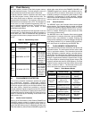
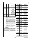
FM1WEn The Flash Memory 1 Write Enable n bits con-
trol write protection for a section of a flash
memory data block. The address mapping of
the register bits is shown below.
15 8 7 0
Reserved IBA
15 0
IBD
15 0
FM0WE
Bit Logical Address Range
0 00 0000h–00 1FFFh
1–14 . . .
15 01 E000h–01 FFFFh
15 0
FM1WE
Bit Logical Address Range
0 02 0000h
–02 1FFFh
1
–14 . . .
15 03 E000h–03 FFFFh


