73 www.national.com
CP3BT26
transmitter circuit of the radio chip is enabled, correspond-
ing to the settings of the power control register in the radio
chip.
The RFSYNC signal is the alternate function of the general-
purpose I/O pin PG0. At reset, this pin is in TRI-STATE
mode. Software must enable the alternate function of the
PG0 pin to give control over this signal to the RF interface.
RFCE
The RFCE signal is the chip enable output to the external
RF chip. When the RFCE signal is driven high, the RF chip
power is controlled by the settings of its power control reg-
isters. When the RFCE signal is driven low, the RF chip is
powered-down. However, the serial interface is still opera-
tional and the CP3BT26 can still access the RF chip internal
control registers.
The RFCE signal is the alternate function of the general-
purpose I/O pin PG1. At reset, this pin is in TRI-STATE
mode. Software must enable the alternate function of the
PG1 pin to give control over this signal to the RF interface.
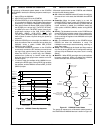
During Bluetooth power-down phases, the CP3BT26 pro-
vides a mechanism to reduce the power consumption of an
external RF chip by driving the RFCE signal of the RF inter-
face to a logic low level. This feature is available when the
Power Management Module of the CP3BT26 has enabled
the Hardware Clock Control mechanism. (However, the cur-
rent version of the radio chip does not implement a power-
reduction mode.)
SCLK
The SCLK signal is the serial interface shift clock output.
The CP3BT26 always acts as the master of the serial inter-
face and therefore always provides the shift clock. The
SCLK signal is the alternate function of the general-purpose
I/O pin PG3. At reset, this pin is in TRI-STATE mode. Soft-
ware must enable the alternate function of the PG3 pin to
give control over this signal to the RF interface.
SDAT
The SDAT signal is the multiplexed serial data receive and
transmit path between the radio chip and the CP3BT26.
The SDAT signal is the alternate function of the general-pur-
pose I/O pin PG4. At reset, this pin is in TRI-STATE mode.
Software must enable the alternate function of the PG4 pin
to give control over this signal to the RF interface.
SLE
The SLE pin is the serial load enable output of the serial in-
terface of the CP3BT26.
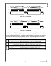
During write operations (to the radio chip registers), the data
received by the shift register of the radio chip is copied into
the address register on the next rising edge of SCLK after
the SLE
signal goes high.
During read operations (read from the registers), the radio
chip releases the SDAT line on the next rising edge of SCLK
after the SLE
signal goes high.
SLE
is the alternate function of the general-purpose I/O pin
PG5. At reset, this pin is in TRI-STATE mode. Software must
enable the alternate function of the PG5 pin to give control
over this signal to the RF interface.
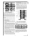
BTSEQ[3:1]
The BTSEQ[3:1] signals indicate internal states of the Blue-
tooth sequencer, which are used for interfacing to some ex-
ternal devices.
15.2 SERIAL INTERFACE
The radio chip register set can be accessed by the
CP3BT26 through the serial interface. The serial interface
uses three pins of the RF interface: SDAT, SCLK, and SLE
.
The serial interface of the CP3BT26 always operates as the
master, providing the shift clock (SCLK) and load enable
(SLE
) signal to the radio chip. The radio chip always acts as
the slave.
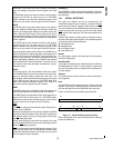
A 25-bit shift protocol is used to perform read/write access-
es to the radio chip internal registers. The complete protocol
is comprised of the following sections:
3-bit Header Field
Read/Write Bit
5-bit Address Field
16-bit Data Field
Header
The 3-bit header contains the fixed data 101b (except for
Fast Write Operations).
Read/Write Bit
The header is followed by the read/write control bit (R/W). If
the Read/Write bit is clear, a write operation is performed
and the 16-bit data portion is copied into the addressed ra-
dio chip register.
Address
The address field is used to select one of the radio chip in-
ternal registers.
Data
The data field is used to transfer data to or from a radio chip
register. The timing is modified for reads, to transfer control
over the data signal from the CP3BT26 to the radio chip.
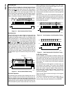
Figure 13 shows the serial interface protocol format.
Figure 13. Serial Interface Protocol Format
Data is transferred on the serial interface with the most sig-
nificant bit (MSB) first.
15 0
Data[15:0]
24 22 21 20 16
Header[2:0] R/W Address[4:0]


