www.national.com 160
CP3BT26
The CVSD/PCM module only supports indirect DMA trans-
fers. Therefore, transferring PCM data between the CVSD/
PCM module and another on-chip module requires two bus
cycles.
The trigger for DMA may also trigger an interrupt if the cor-
responding enable bits in the CVCTRL register is set.
Therefore care must be taken when setting the desired in-
terrupt and DMA enable bits. The following conditions must
be avoided:
Setting the PCMINT bit and either of the DMAPO or
DMAPI bits.
Setting the CVSDINT bit and either of the DMACO or
DMACI bits.
21.8 FREEZE
The CVSD/PCM module provides support for an In-System-
Emulator by means of a special FREEZE input. While
FREEZE is asserted the module will exhibit the following be-
havior:
CVSD In FIFO will not have data removed by the con-
verter core.
CVSD Out FIFO will not have data added by the convert-
er core.
PCM Out buffer will not be updated by the converter
core.
The Clear-on-Read function of the following status bits in
the CVSTAT register is disabled:
PCMINT
CVE
CVF
21.9 CVSD/PCM CONVERTER REGISTERS
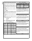
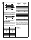
Table 68 lists the CVSD/PCM registers.
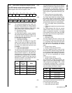
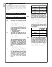
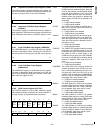
21.9.1 CVSD Data Input Register (CVSDIN)
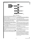
The CVSDIN register is a 16-bit wide, write-only register. It
is used to write CVSD data into the CVSD to PCM converter
FIFO. The FIFO is 8 words deep. The CVSDIN bit 15 repre-
sents the CVSD data bit at t = t
0
, CVSDIN bit 0 represents
the CVSD data bit at t = t
0
- 250 ms.
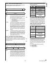
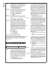
21.9.2 CVSD Data Output Register (CVSDOUT)
The CVSDOUT register is a 16-bit wide read-only register.
It is used to read the CVSD data from the PCM to CVSD
converter. The FIFO is 8 words deep. Reading the CVSD-
OUT register after reset returns undefined data.
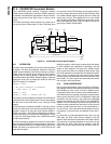
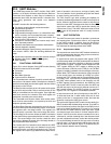
21.9.3 PCM Data Input Register (PCMIN)
The PCMIN register is a 16-bit wide write-only register. It is
used to write PCM data to the PCM to CVSD converter via
the peripheral bus. It is double-buffered, providing a 125 µs
period for an interrupt or DMA request to respond.
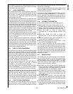
21.9.4 PCM Data Output Register (PCMOUT)
The PCMOUT register is a 16-bit wide read-only register. It
is used to read PCM data from the CVSD to PCM converter.
It is double-buffered, providing a 125 µs period for an inter-
rupt or DMA request to respond. After reset the PCMOUT
register is clear.
Table 68 CVSD/PCM Registers
Name Address Description
CVSDIN FF FC20h
CVSD Data Input
Register
CVSDOUT FF FC22h
CVSD Data Output
Register
PCMIN FF FC24h
PCM Data Input
Register
PCMOUT FF FC26h
PCM Data Output
Register
LOGIN FF FC28h
Logarithmic PCM
Data Input Register
LOGOUT FF FC2Ah
Logarithmic PCM
Data Output Register
LINEARIN FF FC2Ch
Linear PCM
Data Input Register
LINEAROUT FF FC2Eh
Linear PCM
Data Output Register
CVCTRL FF FC30h
CVSD Control Regis-
ter
CVSTAT FF FC32h CVSD Status Register
15 0
CVSDIN
15 0
CVSDOUT
15 0
PCMIN
15 0
PCMOUT
Table 68 CVSD/PCM Registers
Name Address Description


