25 www.national.com
CP3BT26
6.2 BUS INTERFACE UNIT (BIU)
The BIU controls the interface between the CPU core bus
and those on-chip modules which are mapped into BIU
zones. These on-chip modules are the flash program mem-
ory and the I/O zone. The BIU controls the configured pa-
rameters for bus access (such as the number of wait states
for memory access) and issues the appropriate bus signals
for the requested access.
6.3 BUS CYCLES
There are four types of data transfer bus cycles:
Normal read
Fast read
Early write
Late write
The type of data cycle used in a particular transaction de-
pends on the type of CPU operation (a write or a read), the
type of memory or I/O being accessed, and the access type
programmed into the BIU control registers (early/late write
or normal/fast read).
For read operations, a basic normal read takes two clock cy-
cles, and a fast-read bus cycle takes one clock cycle. Nor-
mal read bus cycles are enabled by default after reset.
For write operations, a basic late-write bus cycle takes two
clock cycles, and a basic early-write bus cycle takes three
clock cycles. Early-write bus cycles are enabled by default
after reset. However, late-write bus cycles are needed for
ordinary write operations, so this configuration must be
changed by software (see Section 6.4.1).
In certain cases, one or more additional clock cycles are
added to a bus access cycle. There are two types of addi-
tional clock cycles for ordinary memory accesses, called in-
ternal wait cycles (TIW) and hold (T
hold
) cycles.
A wait cycle is inserted in a bus cycle just after the memory
address has been placed on the address bus. This gives the
accessed memory more time to respond to the transaction
request.
A hold cycle is inserted at the end of a bus cycle. This holds
the data on the data bus for an extended number of clock cy-
cles.
6.4 BIU CONTROL REGISTERS
The BIU has a set of control registers that determine how
many wait cycles and hold cycles are to be used for access-
ing memory. During initialization of the system, these regis-
ters should be programmed with appropriate values so that
the minimum allowable number of cycles is used. This num-
ber varies with the clock frequency.
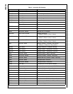
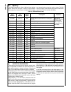
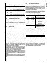
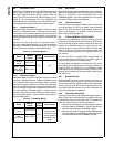
There are five BIU control registers, as listed in Table 8.
These registers control the bus cycle configuration used for
accessing the various on-chip memory types.
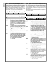
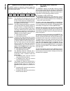
6.4.1 BIU Configuration Register (BCFG)
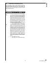
The BCFG register is a byte-wide, read/write register that
selects early-write or late-write bus cycles. At reset, the reg-
ister is initialized to 07h. The register format is shown below.
EWR The Early Write bit controls write cycle timing.
0
– Late-write operation (2 clock cycles to
write).
1
– Early-write operation.
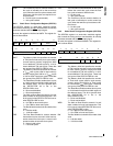
At reset, the BCFG register is initialized to 07h, which se-
lects early-write operation. However, late-write operation is
required for normal device operation, so software must
change the register value to 06h. Bits 1 and 2 of this register
must always be set when writing to this register.
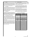
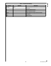
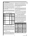
Table 7 Operating Environment Selection
ENV[2:0] EMPTY Operating Environment
111 No Internal ROM enabled (IRE) mode
011 No External ROM enabled (ERE) mode
000 N/A Development (DEV) mode
001 N/A
Development (DEVINT) mode with
internal memory
110 N/A In-System-Programming (ISP) mode
111 Yes In-System-Programming (ISP) mode
011 Yes In-System-Programming (ISP) mode
Table 8 Bus Control Registers
Name Address Description
BCFG FF F900h BIU Configuration Register
IOCFG FF F902h
I/O Zone Configuration
Register
SZCFG0 FF F904h
Static Zone 0
Configuration Register
SZCFG1 FF F906h
Static Zone 1
Configuration Register
SZCFG2 FF F908h
Static Zone 2
Configuration Register
7 3 2 1 0
Reserved 1 1 EWR


