www.national.com 140
CP3BT26
DRIVE The Drive bit shows the output value on the
CANTX pin at the time of the error. Note that
a receiver will not drive the bus except during
ACK and during an active error flag.
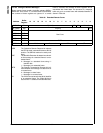
19.10.17 CAN Timer Register (CTMR)
The CTMR register reports the current value of the Time
Stamp Counter as described in Section 19.8.
The CTMR register is a free running 16-bit counter. It con-
tains the number of CAN bits recognized by the CAN mod-
ule since the register has been cleared. The counter starts
to increment from the value 0000b after a hardware reset. If
the Timer Stamp Enable bit (TSTPEN) in the CAN global
configuration register (CGCR) is set, the counter will also be
cleared on a message transfer of the message buffer 0.
The contents of CTMR are captured into the Time Stamp
register of the message buffer after successfully sending or
receiving a frame, as described in “Time Stamp Counter” on
page 126.
19.11 SYSTEM START-UP AND MULTI-INPUT
WAKE-UP
After system start-up, all CAN-related registers are in their
reset state. The CAN module can be enabled after all con-
figuration registers are set to their desired value. The follow-
ing initial settings must be made:
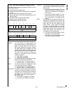
Configure the CAN Timing register (CTIM). See “Bit
Time Logic” on page 117.
Configure every buffer to its function as receive/transmit.
See “Buffer Status/Control Register (CNSTAT)” on
page 128.
Set the acceptance filtering masks. See “Acceptance Fil-
tering” on page 119.
Enable the CAN interface. See “CAN Global Configura-
tion Register (CGCR)” on page 133.
Before disabling the CAN module, software must make sure
that no transmission is still pending.
Note: Activity on the CAN bus can wake up the device from
a reduced-power mode by selecting the CANRX pin as an
input to the Multi-Input Wake-Up module. In this case, the
CAN module must not be disabled before entering the re-
duced-power mode. Disabling the CAN module also dis-
ables the CANRX pin. As an alternative, the CANRX pin can
be connected to any other input pin of the Multi-Input Wake-
Up module. This input channel must then be configured to
trigger a wake-up event on a falling edge (if a dominant bit
is represented by a low level). In this case, the CAN module
can be disabled before entering the reduced-power mode.
After waking up, software must enable the CAN module
again. All configuration and buffer registers still contain the
same data they held before the reduced-power mode was
entered.
19.11.1 External Connection
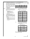
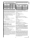
The CAN module uses the CANTX and CANRX pins to con-
nect to the physical layer of the CAN interface. They provide
the functionality described in Table 64.
The logic levels are configurable by the CTX and CRX bits
of the Global Configuration Register CGCR (see “CAN Glo-
bal Configuration Register (CGCR)” on page 133).
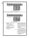
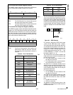
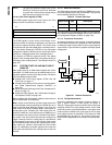
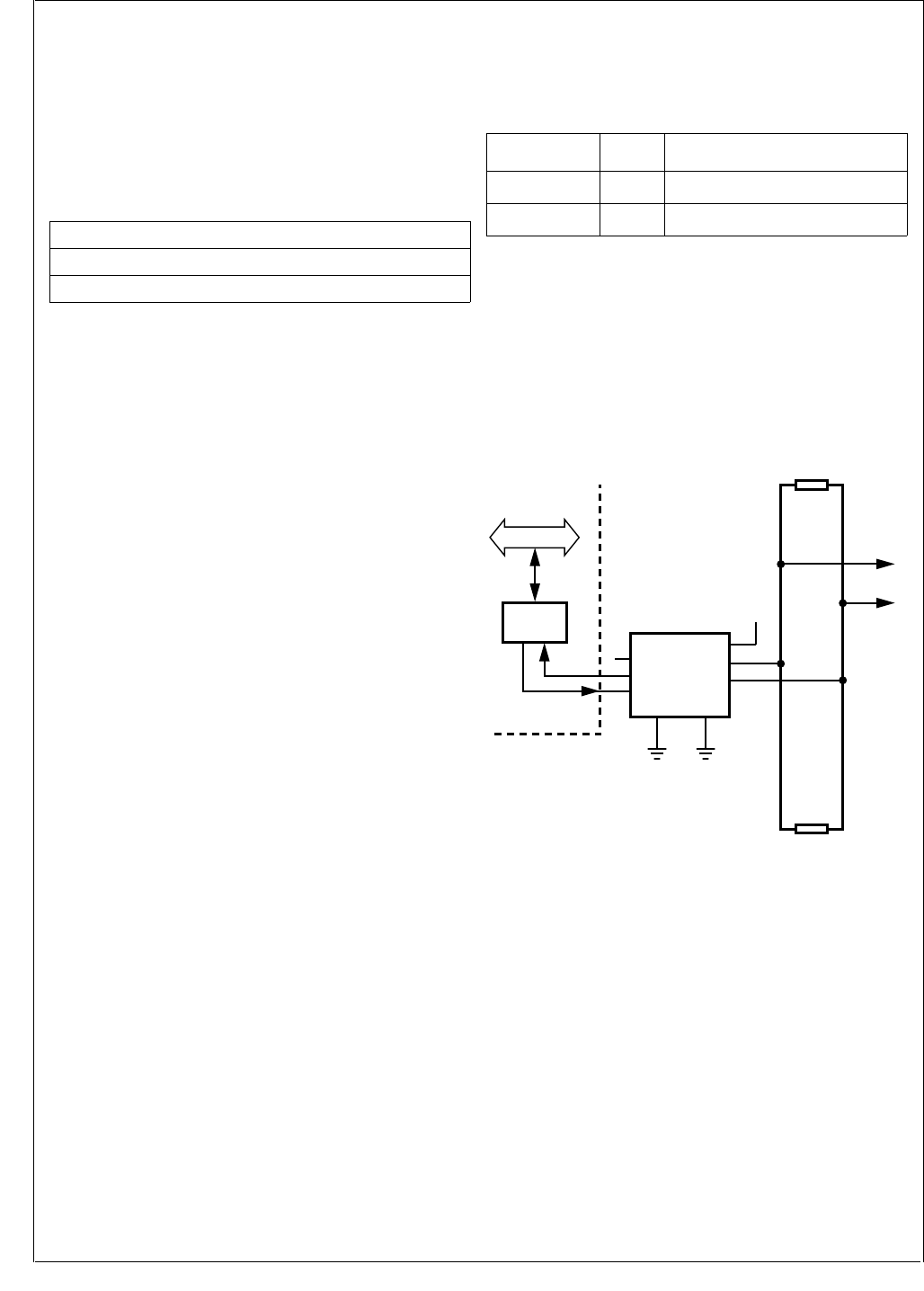
19.11.2 Transceiver Connection
An external transceiver chip must be connected between
the CAN block and the bus. It establishes a bus connection
in differential mode and provides the driver and protection
requirements. Figure 64 shows a possible ISO-High-Speed
configuration
.
Figure 64. External Transceiver
19.11.3 Timing Requirements
Processing messages and updating message buffers re-
quire a certain number of clock cycles, as shown in
Table 65. These requirements may lead to some restrictions
regarding the Bit Time Logic settings and the overall CAN
performance which are described below in more detail. Wait
cycles need to be added to the cycle count for CPU access
to the object memory as described in CPU Access to CAN
Registers/Memory on page 127. The number of occurrenc-
es per frame is dependent on the number of matching iden-
tifiers.
15 0
CTMR15:0
0
R
Table 64 External CAN Pins
Signal Name Type Description
CANTX Output Transmit data to the CAN bus
CANRX Input Receive data from the CAN bus
CR16CAN
CANRX
CANTX
5
REF
4
RX
1
TX
VCC
VCC
To other
modules
CAN bus
signals
Termination
3
BUS_H
7
BUS_L
6
RS
8
CPU Bus
GND
Transceiver Chip
120
120
2
DS048


