www.national.com 28
CP3BT26
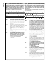
FRE The Fast Read Enable bit controls whether
fast read bus cycles are used. A fast read op-
eration takes one clock cycle. A normal read
operation takes at least two clock cycles.
0
– Normal read cycles.
1 – Fast read cycles.
IPST The Post Idle bit controls whether an idle cycle
follows the current bus cycle, when the next
bus cycle accesses a different zone.
0
– No idle cycle.
1
– Idle cycle inserted.
IPRE The Preliminary Idle bit controls whether an
idle cycle is inserted prior to the current bus
cycle, when the new bus cycle accesses a dif-
ferent zone.
0
– No idle cycle.
1 – Idle cycle inserted.
6.5 WAIT AND HOLD STATES
The number of wait cycles and hold cycles inserted into a
bus cycle depends on whether it is a read or write operation,
the type of memory or I/O being accessed, and the control
register settings.
6.5.1 Flash Program/Data Memory
When the CPU accesses the Flash program and data mem-
ory (address ranges 000000h
–03FFFFh and 0E0000h–
0E1FFFh), the number of added wait and hold cycles de-
pends on the type of access and the BIU register settings.
In fast-read mode (SZCFG0.FRE=1), a read operation is a
single cycle access. This limits the maximum CPU operat-
ing frequency to 24 MHz.
For a read operation in normal-read mode
(SZCFG0.FRE=0), the number of inserted wait cycles is
specified in the SZCFG0.WAIT field. The total number of
wait cycles is the value in the WAIT field plus 1, so it can
range from 1 to 8. The number of inserted hold cycles is
specified in the SCCFG0.HOLD field, which can range from
0 to 3.
For a write operation in fast read mode (SZCFG0.FRE=1),
the number of inserted wait cycles is 1. No hold cycles are
used.
For a write operation normal read mode (SZCFG0.FRE=0),
the number of wait cycles is equal to the value written to the
SZCFG0.WAIT field plus 1 (in the late write mode) or 2 (in
the early write mode). The number of inserted hold cycles is
equal to the value written to the SCCFG0.HOLD field, which
can range from 0 to 3.
6.5.2 RAM Memory
Read and write accesses to on-chip RAM is performed with-
in a single cycle, without regard to the BIU settings. The
RAM address is in the range of 0E 0000h
–0E 7FFFh and 0E
8000h–0E 91FFh.
6.5.3 Access to Peripherals
When the CPU accesses on-chip peripherals in the range of
0E F000h
–0E F1FFh and FF 0000h–FF FBFFh, one wait
cycle and one preliminary idle cycle is used. No hold cycles
are used. The IOCFG register determines the access timing
for the address range FF FB00h
–FF FBFFh.


