133 www.national.com
CP3BT26
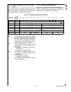
19.10.6 CAN Global Configuration Register (CGCR)
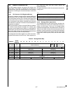
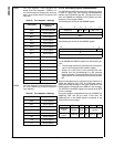
The CAN Global Configuration Register (CGCR) is a 16-bit
wide register used to:
Enable/disable the CAN module.
Configure the BUFFLOCK function for the message buff-
er 0..14.
Enable/disable the time stamp synchronization.
Set the logic levels of the CAN Input/Output pins, CAN-
RX and CANTX.
Choose the data storage direction (DDIR).
Select the error interrupt type (EIT).
Enable/disable diagnostic functions.
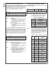
CANEN The CAN Enable bit enables/disables the
CAN module. When the CAN module is dis-
abled, all internal states and the TEC and
REC counter registers are cleared. In addition
the CAN module clock is disabled. All CAN
module control registers and the contents of
the object memory are left unchanged. Soft-
ware must make sure that no message is
pending for transmission before the CAN
module is disabled.
0 – CAN module is disabled.
1 – CAN module is enabled.
CTX The Control Transmit bit configures the logic
level of the CAN transmit pin CANTX.
0 – Dominant state is 0; recessive state is 1.
1 – Dominant state is 1; recessive state is 0.
CRX The Control Receive bit configures the logic
level of the CAN receive pin CANRX.
0 – Dominant state is 0; recessive state is 1.
1 – Dominant state is 1; recessive state is 0.
BUFFLOCK The Buffer Lock bit configures the buffer lock
function. If this feature is enabled, a buffer will
be locked upon a successful frame reception.
The buffer will be unlocked again by writing
RX_READY in the buffer status register, i.e.,
after reading data.
0 – Lock function is disabled for all buffers.
1 – Lock function is enabled for all buffers.
TSTPEN The Time Sync Enable bit enables or disables
the time stamp synchronization function of the
CAN module.
0 – Time synchronization disabled. The Time
Stamp counter value is not reset upon re-
ception or transmission of a message to/
from buffer 0.
1 – Time synchronization enabled. The Time
Stamp counter value is reset upon recep-
tion or transmission of a message to/from
buffer 0.
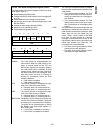
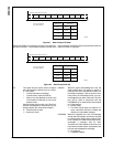
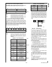
DDIR The Data Direction bit selects the direction the
data bytes are transmitted and received. The
CAN module transmits and receives the CAN
Data1 byte first and the Data8 byte last
(Data1, Data2,...,Data7, Data8). If the DDIR
bit is clear, the data contents of a received
message is stored with the first byte at the
highest data address and the last data at the
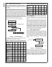
lowest data address (see Figure 61). The
same applies for transmitted data.
0 – First byte at the highest address, subse-
quent bytes at lower addresses.
1 – First byte at the lowest address, subse-
quent bytes at higher addresses.
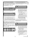
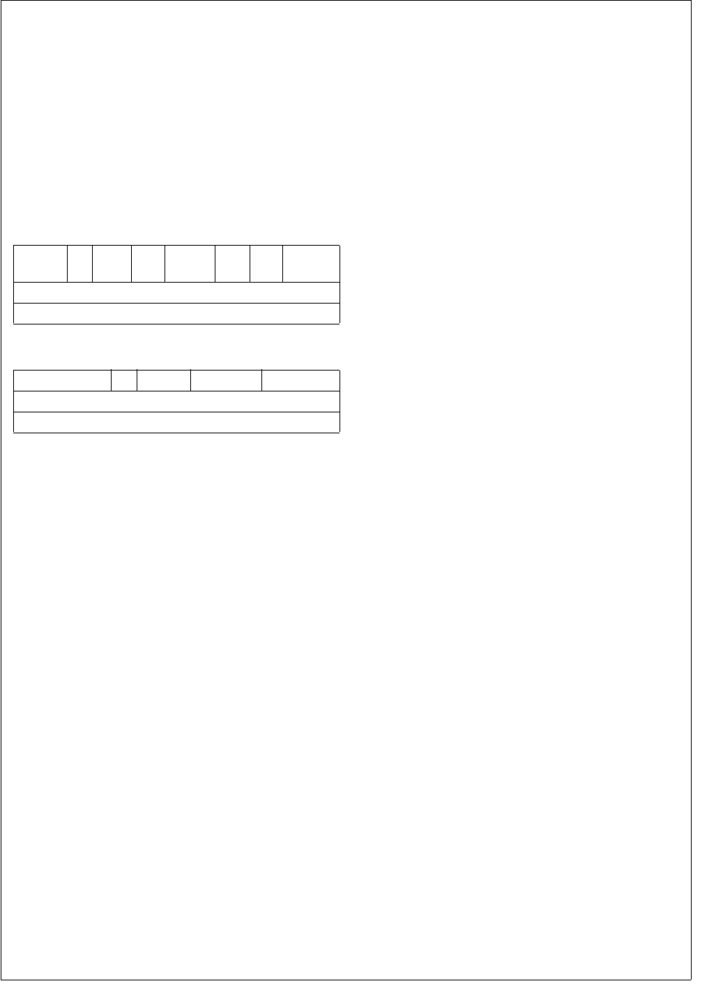
7 6 5 4 3 2 1 0
IGNACK LO DDIR
TST
PEN
BUFF
LOCK
CRX CTX CANEN
0
R/W
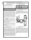
15 12 11 10 9 8
Reserved EIT DIAGEN INTERNAL LOOPBACK
0
R/W


