www.national.com 86
CP3BT26
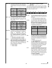
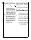
16.5.3 ADC Conversion Control Register
(ADCCNTRL)
The ADCCNTRL register specifies the trigger conditions for
an ADC conversion.
POL The ASYNC Polarity bit specifies the polarity
of edges which trigger ADC conversions.
0 – ASYNC input is sensitive to rising edges.
1 – ASYNC input is sensitive to falling edges.
EXT The External Trigger bit selects whether con-
versions are triggered by writing the ADC-
START register or activity on the ASYNC
input.
0 – ADC conversions triggered by writing to
the ADCSTART register.
1 – ADC conversions triggered by qualified
edges on ASYNC input.
AUTO The Automatic bit controls whether automatic
mode is enabled, in which any qualified edge
on the ASYNC input is recognized as a trigger
event. When automatic mode is disabled, the
ADC module must be “primed” before a qual-
ified edge on the ASYNC input can trigger a
conversion. To prime the ADC module, soft-
ware must write the ADCSTART register with
any value before an edge on the ASYNC input
is recognized as a trigger event. After the con-
version is completed, the ASYNC input will be
ignored until software again writes the ADC-
START register. The AUTO bit is ignored
when the EXT bit is 0.
0 – Automatic mode disabled.
1 – Automatic mode enabled.
16.5.4 ADC Start Conversion Register (ADCSTART)
The ADCSTART register is a write-only register used by
software to initiate an ADC conversion. Writing any value to
this register will cause the ADC to initiate a conversion or
prime the ADC to initiate a conversion, as controlled by the
ADCCNTRL register.
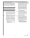
16.5.5 ADC Start Conversion Delay Register
(ADCSCDLY)
The ADCSCDLY register controls critical timing parameters
for the operation of the ADC module.
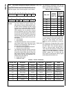
ADC_DELAY2
The ADC Delay 2 field specifies the delay be-
tween the ADC module clock source (either
System Clock after a programmable divider or
Auxiliary Clock 2) and the ADC clock. The
range of effective values for this field is 0 to
20. Values above 20 produce the same delay
as 20, which is about 42 ns.
ADC_DELAY1
The ADC Delay 1 field specifies the number of
clock periods by which the trigger event will be
delayed before initiating a conversion. The
timebase for this delay is the ADC clock (12
MHz) divided by the ADC_DIV divisor. The
ADC_DELAY1 field has 9 bits, which corre-
sponds to a maximum delay of 511 clock peri-
ods.
ADC_DIV The ADC Clock Divisor field specifies the divi-
sor applied to the ADC clock (12 MHz) to gen-
erate the clock used to drive the DELAY1
block. A field value of n results in a division ra-
tio of n+1. With a module clock of 12 MHz, the
maximum delay which can be provided by
ADC_DIV and ADC_DELAY settings is:
15 3 2 1 0
Reserved AUTO EXT POL
15 14 13 5 4 0
ADC_DIV ADC_DELAY1 ADC_DELAY2
1
12 MHz
--------------------
4× 511× 170 us=


