161 www.national.com
CP3BT26
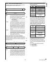
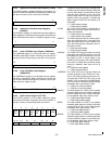
21.9.5 Logarithmic PCM Data Input Register (LOGIN)
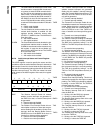
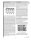
The LOGIN register is an 8-bit wide write-only register. It is
used to receive 8-bit logarithmic PCM data from the periph-
eral bus and convert it into 13-bit linear PCM data.
21.9.6 Logarithmic PCM Data Output Register
(LOGOUT)
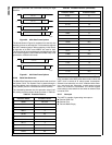
The LOGOUT register is an 8-bit wide read-only register. It
holds logarithmic PCM data that has been converted from
linear PCM data. After reset, the LOGOUT register is clear.
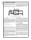
21.9.7 Linear PCM Data Input Register (LINEARIN)
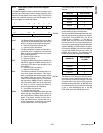
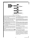
The LINEARIN register is a 16-bit wide write-only register.
The data is left-aligned. When converting to A-law, bits 2:0
are ignored. When converting to µ-law, bits 1:0 are ignored.
21.9.8 Linear PCM Data Output Register
(LINEAROUT)
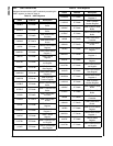
The LINEAROUT register is a 16-bit wide read-only register.
The data is left-aligned. When converting from A-law, bits
2:0 are clear. When converting from µ-law, bits 1:0 are clear.
After reset, this register is clear.
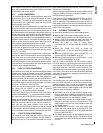
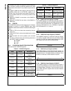
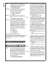
21.9.9 CVSD Control Register (CVCTRL)
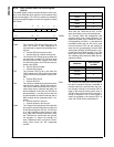
The CVCTRL register is a 16-bit wide, read/write register
that controls the mode of operation and of the module’s in-
terrupts. At reset, all implemented bits are cleared.
CVEN The Module Enable bit enables or disables the
CVSD conversion module interface. When the
bit is set, the interface is enabled which allows
read and write operations to the rest of the
module. When the bit is clear, the module is
disabled. When the module is disabled the
status register CVSTAT will be cleared to its
reset state.
0 – CVSD module enabled.
1 – CVSD module disabled.
CLKEN The CVSD Clock Enable bit enables the 2-
MHz clock to the filter engine and CVSD en-
coders and decoders.
0 – CVSD module clock disabled.
1 – CVSD module clock enabled.
PCMINT The PCM Interrupt Enable bit controls gener-
ation of the PCM interrupt
. If set, this bit en-
ables the PCM interrupt. If the PCMINT bit is
clear, the PCM interrupt is disabled. After re-
set, this bit is clear.
0 – PCM interrupt disabled.
1 – PCM interrupt enabled.
CVSDINT The CVSD FIFO Interrupt Enable bit controls
generation of the CVSD interrupt. If set, this
bit enables the CVSD interrupt that occurs if
the CVSD In FIFO is nearly empty or the
CVSD Out FIFO is nearly full. If the CVSDINT
bit is clear, the CVSD nearly full/nearly empty
interrupt is disabled. After reset, this bit is
clear.
0 – CVSD interrupt disabled.
1 – CVSD interrupt enabled.
CVSDERRINT
The CVSD FIFO Error Interrupt Enable bit
controls generation of the CVSD error inter-
rupt. If set, this bit enables an interrupt to oc-
cur when the CVSD Out FIFO is full or the
CVSD In FIFO is empty. If the CVSDERROR-
INT bit is clear, the CVSD full/empty interrupt
is disabled. After reset, this bit is clear.
0 – CVSD error interrupt disabled.
1 – CVSD error interrupt enabled.
DMACO The DMA Enable for CVSD Out bit enables
hardware DMA control for reading CVSD data
from the CVSD Out FIFO. If clear, DMA sup-
port is disabled. After reset, this bit is clear.
0 – CVSD output DMA disabled.
1 – CVSD output DMA enabled.
DMACI The DMA Enable for CVSD In bit enables
hardware DMA control for writing CVSD data
into the CVSD In FIFO. If clear, DMA support
is disabled. After reset, this bit is clear.
0 – CVSD input DMA disabled.
1 – CVSD input DMA enabled.
DMAPO The DMA Enable for PCM Out bit enables
hardware DMA control for reading PCM data
from the PCMOUT register. If clear, DMA sup-
port is disabled. After reset, this bit is clear.
0 – PCM output DMA disabled.
1 – PCM output DMA enabled.
70
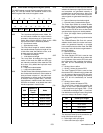
LOGIN
70
LOGOUT
15 0
LINEARIN
15 0
LINEAROUT
7 6 5 4 3 2 1 0
DMA
PO
DMA
CI
DMA
CO
CVSD
ERR-
INT
CVSD
INT
PCM
INT
CLK
EN
CVEN
15 14 13 12 11 10 9 8
Res. RESOLUTION PCMCONV CVSDCONV DMAPI


