31 www.national.com
CP3BT26
8.0 Flash Memory
The flash memory consists of the flash program memory
and the flash data memory. The flash program memory is
further divided into the Boot Area and the Code Area.
A special protection scheme is applied to the lower portion
of the flash program memory, called the Boot Area. The
Boot Area always starts at address 0 and ranges up to a
programmable end address. The maximum boot area ad-
dress which can be selected is 00 77FFh. The intended use
of this area is to hold In-System-Programming (ISP) rou-
tines or essential application routines. The Boot Area is al-
ways protected against CPU write access, to avoid
unintended modifications.
The Code Area is intended to hold the application code and
constant data. The Code Area begins with the next byte af-
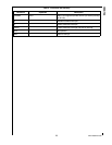
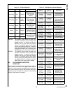
ter the Boot Area. Table 10 summarizes the properties of
the regions of flash memory mapped into the CPU address
space.
Table 10 Flash Memory Areas
8.1 FLASH MEMORY PROTECTION
The memory protection mechanisms provide both global
and section-level protection. Section-level protection
against CPU writes is applied to individual 8K-byte sections
of the flash program memory and 512-byte sections of the
flash data memory. Section-level protection is controlled
through read/write registers mapped into the CPU address
space. Global write protection is applied at the device level,
to disable flash memory writes by the CPU. Global write pro-
tection is controlled by the encoding of bits stored in the
flash memory array.
8.1.1 Section-Level Protection
Each bit in the Flash Memory Write Enable (FM0WER and
FM1WER) registers enables or disables write access to a
corresponding section of flash program memory. Write ac-
cess to the flash data memory is controlled by the bits in the
Flash Slave Memory Write Enable (FSM0WER) register. By
default (after reset) all bits in the FM0WER, FM1WER, and
FSM0WER registers are cleared, which disables write ac-
cess by the CPU to all sections. Write access to a section is
enabled by setting the corresponding write enable bit. After
completing a programming or erase operation, software
should clear all write enable bits to protect the flash program
memory against any unintended writes.
8.1.2 Global Protection
The WRPROT field in the Protection Word controls global
write protection. The Protection Word is located in a special
flash memory outside of the CPU address space. If a major-
ity of the bits in the 3-bit WRPROT field are clear, write pro-
tection is enabled. Enabling this mode prevents the CPU
from writing to flash memory.
The RDPROT field in the Protection Word controls global
read protection. If a majority of the bits in the 3-bit RDPROT
field are clear, read protection is enabled. Enabling this
mode prevents reading by an external debugger through the
serial debug interface or by an external flash programmer.
CPU read access is not affected by the RDPROT bits.
8.2 FLASH MEMORY ORGANIZATION
Each of the flash memories are divided into main blocks and
information blocks. The main blocks hold the code or data
used by application software. The information blocks hold
factory parameters, protection settings, and other device-
specific data. The main blocks are mapped into the CPU ad-
dress space. The information blocks are accessed indirectly
through a register-based interface. Separate sets of regis-
ters are provided for accessing flash program memory (FM
registers) and flash data memory (FSM registers). The flash
program memory consists of two main blocks and two data
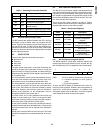
blocks, as shown in Table 11. The flash data memory con-
sists of one main block and one information block.
Table 11 Flash Memory Blocks
Area Address Range
Read
Access
Write Access
Boot
Area
0
–BOOTAREA - 1 Yes No
Code
Area
BOOTAREA–03 FFFFh Yes
Write access
only if section
write enable
bit is set and
global write
protection is
disabled.
Data
Area
0E 0000h
–0E 1FFFh Yes
Write access
only if section
write enable
bit is set and
global write
protection is
disabled.
Name Address Range Function
Main Block 0
00 0000h
–01 FFFFh
(CPU address space)
Flash Program
Memory
Information
Block 0
000h
–07Fh
(address register)
Function Word,
Factory
Parameters
Main Block 1
02 0000h
–03 FFFFh
(CPU address space)
Flash Program
Memory
Information
Block 1
080h
–0FFh
(address register)
Protection Word,
User Data
Main Block 2
0D 0000h
–0D 1FFFh
(CPU address space)
Flash Data
Memory
Information
Block 2
000h
–07Fh
(address register)
User Data


