www.national.com 74
CP3BT26
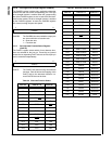
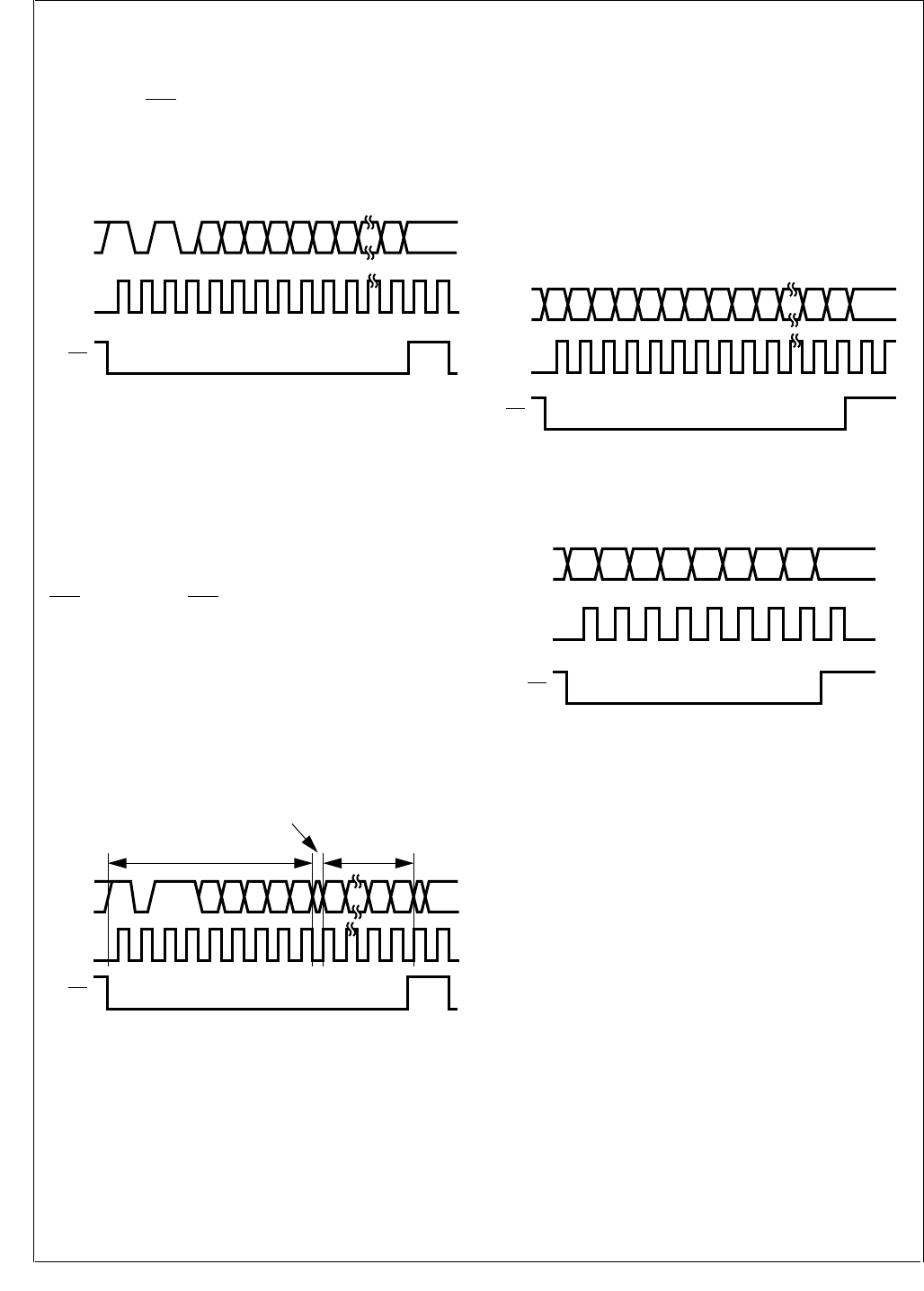
Write Operation
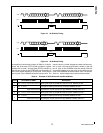
When the R/W bit is clear, the 16 bits of the data field are
shifted out of the CP3BT26 on the falling edge of SCLK.
Data is sampled by the radio chip on the rising edge of
SCLK. When SLE
is high, the 16-bit data are copied into the
radio chip register on the next rising edge of SCLK. The
data is loaded in the appropriate radio chip register depend-
ing on the state of the four address bits, Address[4:0].
Figure 14 shows the timing for the write operation.
Figure 14. Serial Interface Write Timing
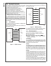
Read Operation
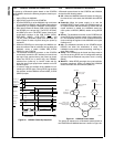
When the R/W bit is set, data is shifted out of the radio chip
on the rising edge of SCLK. Data is sampled by the
CP3BT26 on the falling edge of SCLK. On reception of the
read command (R/W = 1), the radio chip takes control of the
serial interface data line. The received 16-bit data is loaded
by the CP3BT26 after the first falling edge of SCLK when
SLE
is high. When SLE is high, the radio chip releases the
SDAT line again on the next rising edge of SCLK. The
CP3BT26 takes control of the SDAT line again after the fol-
lowing rising edge of SCLK. Which radio chip register is
read, depends on the state of the four address bits, Ad-
dress[4:0]. The transfer is always 16 bits, without regard to
the actual size of the register. Unimplemented bits contain
undefined data. Figure 15 shows the timing for the read op-
eration.
Figure 15. Serial Interface Read Timing
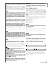
Fast-Write Operation
An enhanced serial interface mode including fast write ca-
pability is enabled when the FW bit in the radio chip is set.
This bit activates a mode with decreased addressing and
control overhead, which allows fast loading of time-critical
registers during normal operation. When the FW bit is set,
the 3-bit header may have a value other than 101b, and it is
used to address the write-only registers of the radio chip.
Fast writes load the same physical register as the corre-
sponding normal write operation.
For the power control and CMOS output registers of the RF
chip, it is only necessary to transmit a total of 8 bits (3 ad-
dress bits and 5 data bits), because the remaining eight bits
are unused.
While the FW bit is set, normal Read/Write operations are
still valid and may be used to access non-time-critical con-
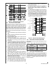
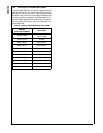
trol registers. Figure 16 shows the timing for a 16-bit Fast-
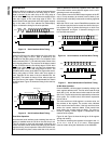
Write transaction, and Figure 17 shows the timing for an 8-
bit Fast-Write transaction.
Figure 16. Serial Interface 16-bit Fast-Write Timing
Figure 17. Serial Interface 8-bit Fast-Write Timing
32-Bit Write Operation
On the LMX5252, a 32-bit register is loaded by writing to the
same register address twice. The first write loads the high
word (bits 31:16), and the second write loads the low word
(bits 15:0). The two writes must be separated by at least two
clock cycles. For a 4-MHz clock, the minimum separation
time is 500 ns.
The value read from a 32-bit register is a counter value, not
the contents of the register. The counter value indicates
which words have been written. If the high word has been
written, the counter reads as 0000h. If both words have
been written, the counter reads as 0001h. The value re-
turned by reading a 32-bit register is independent of the
contents of the register.
Figure 18 and Figure 19 show the timing for 32-bit register
writing and reading.
The order for accessing the registers is from high to low: 17,
15, 14, 12, 11, 10, 9, 8, 7, 6, 5, 4, 2, and 1. These registers
must be written during the initialization of the LMX5252.
D0D14A0A1A2A3A4WH0H1H2 D15
SLE
SCLK
SDAT
DS012
D0D1A0A1A2A3A4RH0H1H2 D15
SLE
SCLK
SDAT
Master drives SDAT
Slave drives SDAT
SDAT Floating
DS013
D8 D7 D6 D1 D0D9D10D11D12A0A1A2
SLE
SCLK
SDAT
DS014
D8D9D10D11D12A0A1A2
SLE
SCLK
SDAT
DS015


