www.national.com 176
CP3BT26
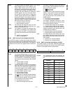
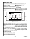
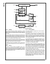
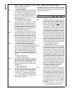
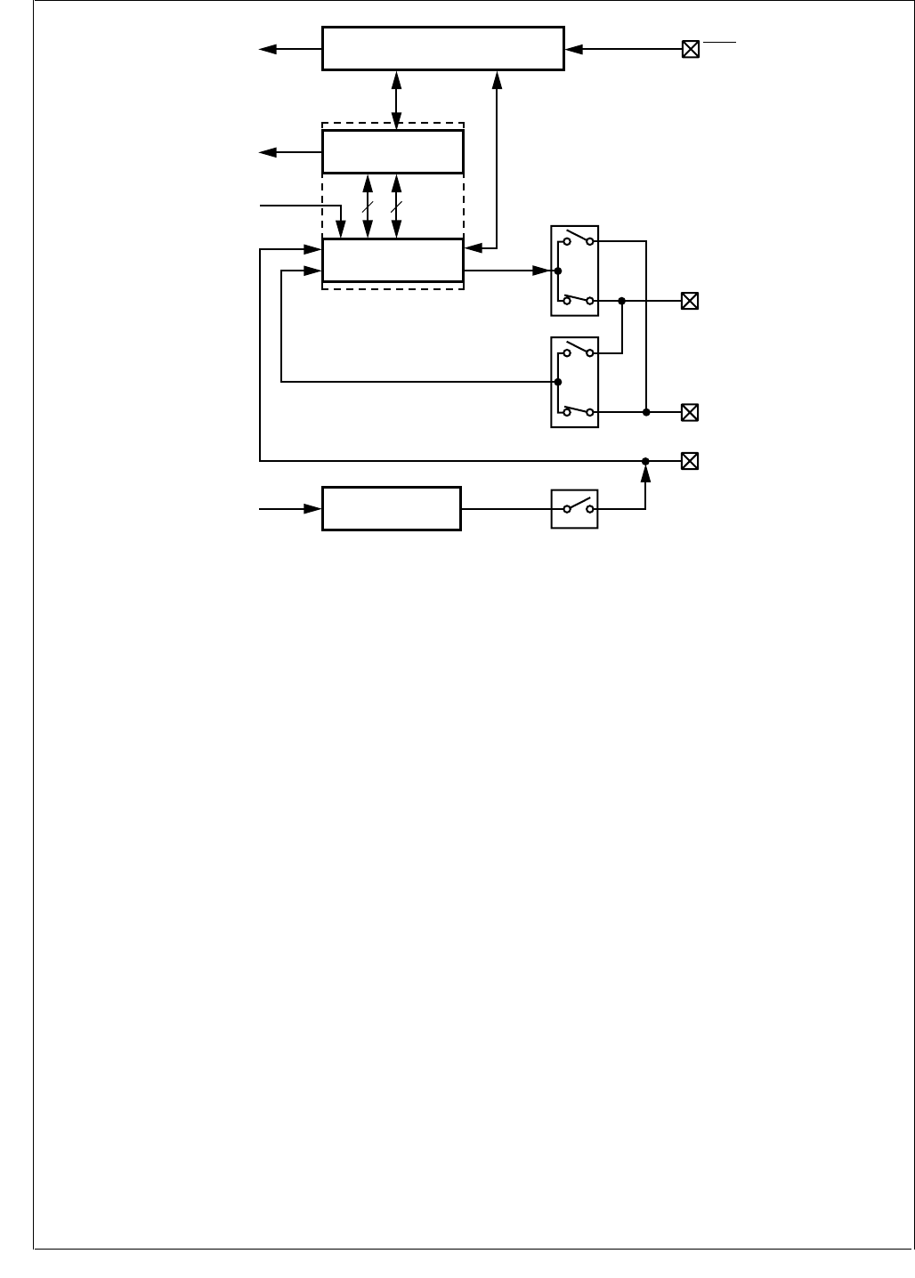
Figure 84. Microwire Block Diagram
23.1.2 Reading
The enhanced Microwire interface implements a double
buffer on read. As illustrated in Figure 84, the double read
buffer consists of the 16-bit shifter and a buffer, called the
read buffer.
The 16-bit shifter loads the read buffer with new data when
the data transfer sequence is completed and previous data
in the read buffer has been read. In master mode, an Over-
run error occurs when the read buffer is full, the 16-bit shifter
is full and a new data transfer sequence starts.
When 8-bit mode is selected, the lower byte of the shift reg-
ister is loaded into the lower byte of the read buffer and the
read buffer’s higher byte remains unchanged.
The RBF bit indicates if the MWDAT register holds valid da-
ta. The OVR bit indicates that an overrun condition has oc-
curred.
23.1.3 Writing
The BSY bit indicates whether the MWDAT register can be
written. All write operations to the MWDAT register update the
shifter while the data contained in the read buffer is not affect-
ed. Undefined results will occur if the MWDAT register is writ-
ten to while the BSY bit is set.
23.1.4 Clocking Modes
Two clocking modes are supported: the normal mode and
the alternate mode.
In the normal mode, the output data, which is transmitted on
the MDODI pin (master mode) or the MDIDO pin (slave
mode), is clocked out on the falling edge of the shift clock
MSK. The input data, which is received via the MDIDO pin
(master mode) or the MDODI pin (slave mode), is sampled
on the rising edge of MSK.
In the alternate mode, the output data is shifted out on the
rising edge of MSK on the MDODI pin (master mode) or
MDIDO pin (slave mode). The input data, which is received
via MDIDO pin (master mode) or MDODI pin (slave mode),
is sampled on the falling edge of MSK.
The clocking modes are selected with the SCM bit. The
SCIDL bit allows selection of the value of MSK when it is idle
(when there is no data being transferred). Various MSK
clock frequencies can be programmed via the MCDV bits.
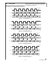
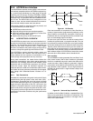
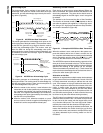
Figures Figure 85, Figure 86, Figure 87, and Figure 88 show
the data transfer timing for the normal and the alternate
modes with the SCIDL bit clear and set.
Note that when data is shifted out on MDODI (master mode)
or MDIDO (slave mode) on the leading edge of the MSK
clock, bit 14 (16-bit mode) is shifted out on the second lead-
ing edge of the MSK clock. When data are shifted out on
MDODI (master mode) or MDIDO (slave mode) on the trail-
ing edge of MSK, bit 14 (16-bit mode) is shifted out on the
first trailing edge of MSK.
16-BIt Shift Register
Write
Data
Write
Data
Clock Prescaler + Select
16-BIt Read Buffer
Control + Status
Slave
Master
MWDAT
MWCS
MDODI
MSK
Interrupt
Request
System
Clock
Data Out
Data In
MSK
88
Slave
Master
Master
MDIDO
DS068


