165 www.national.com
CP3BT26
22.2.2 Synchronous Mode
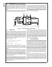
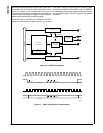
The synchronous mode of the UART enables the device to
communicate with other devices using three communication
signals: transmit, receive, and clock. In this mode, data bits
are transferred synchronously with the UART clock signal.
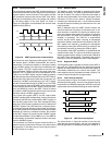
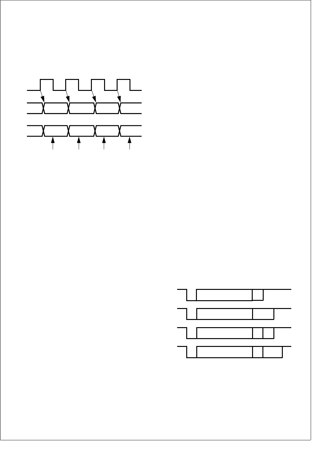
Data bits are transmitted on the rising edges and received
on the falling edges of the clock signal, as shown in
Figure 78. Data bytes are transmitted and received least
significant bit (LSB) first.
Figure 78. UART Synchronous Communication
In synchronous mode, the transmit shift register (TSFT) and
the transmit buffer (UnTBUF) double-buffer the data for
transmission. To transmit a character, a data byte is loaded
in the UnTBUF register. The data is then transferred to the
TSFT register. The TSFT register shifts out one bit of the
current character, LSB first, on each rising edge of the clock.
While the TSFT is shifting out the current character on the
TXD pin, the UnTBUF register may be loaded by software
with the next byte to be transmitted. When the TSFT finishes
transmission of the last stop bit within the current frame, the
contents of UnTBUF are transferred to the TSFT register
and the Transmit Buffer Empty bit (UTBE) is set. The UTBE
bit is automatically reset by the UART when software loads
a new character into the UnTBUF register. During transmis-
sion, the UXMIP bit is set by the UART. This bit is cleared
only after the UART has sent the last frame bit of the current
character and the UnTBUF register is empty.
The receive shift register (RSFT) and the receive buffer
(URBUF) double-buffer the data being received. Serial data
received on the RXD pin is shifted into the RSFT register on
the first falling edge of the clock. Each subsequent falling
edge of the clock causes an additional bit to be shifted into
the RSFT register. The UART assumes a complete charac-
ter has been received after the correct number of rising edg-
es on CKX (based on the selected frame format) have been
detected. On receiving a complete character, the contents
of the RSFT register are copied into the UnRBUF register
and the Receive Buffer Full bit (URBF) is set. The URBF bit
is automatically cleared when software reads the character
from the UnRBUF register.
The transmitter and receiver may be clocked by either an
external source provided to the CKX pin or the internal baud
rate generator. In the latter case, the clock signal is placed
on the CKX pin as an output.
22.2.3 Attention Mode
The Attention mode is available for networking this device
with other processors. This mode requires the 9-bit data for-
mat with no parity. The number of start bits and number of
stop bits are programmable. In this mode, two types of 9-bit
characters are sent on the network: address characters
consisting of 8 address bits and a 1 in the ninth bit position
and data characters consisting of 8 data bits and a 0 in the
ninth bit position.
While in Attention mode, the UART receiver monitors the
communication flow but ignores all characters until an ad-
dress character is received. On receiving an address char-
acter, the contents of the receive shift register are copied to
the receive buffer. The URBF bit is set and an interrupt (if
enabled) is generated. The UATN bit is automatically
cleared, and the UART begins receiving all subsequent
characters. Software must examine the contents of the UR-
BUF register and respond by accepting the subsequent
characters (by leaving the UATN bit clear) or waiting for the
next address character (by setting the UATN bit again).
The operation of the UART transmitter is not affected by the
selection of this mode. The value of the ninth bit to be trans-
mitted is programmed by setting or clearing the UXB9 bit in
the UART Frame Select register. The value of the ninth bit
received is read from URB9 in the UART Status Register.
22.2.4 Diagnostic Mode
The Diagnostic mode is available for testing of the UART. In
this mode, the TXD and RXD pins are internally connected
together, and data shifted out of the transmit shift register is
immediately transferred to the receive shift register. This
mode supports only the 9-bit data format with no parity. The
number of start and stop bits is programmable.
22.2.5 Frame Format Selection
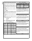
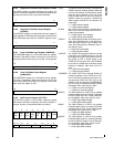
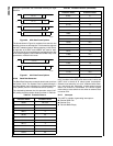
The format shown in Figure 79 consists of a start bit, seven
data bits (excluding parity), and one or two stop bits. If parity
bit generation is enabled by setting the UPEN bit, a parity bit
is generated and transmitted following the seven data bits.
Figure 79. 7-Bit Data Frame Options
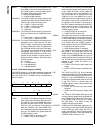
The format shown in Figure 80 consists of one start bit,
eight data bits (excluding parity), and one or two stop bits. If
parity bit generation is enabled by setting the UPEN bit, a
CKX
TDX
RDX
Sample Input
DS062
1
Start
Bit
7-Bit Data 1S
1a
Start
Bit
7-Bit Data 2S
1b
Start
Bit
7-Bit Data 1SPA
1c
Start
Bit
7-Bit Data 2SPA
DS063


