93 www.national.com
CP3BT26
Receive Endpoint FIFO Operation (RXFIFO1, RXFIFO2,
RXFIFO3)
The Receive FIFOs for endpoints 2, 4, and 6 support bulk,
interrupt, and isochronous USB packet transfers larger than
the actual FIFO size. If the packet length exceeds the FIFO
size, software must read the FIFO contents while the USB
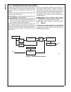
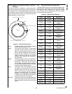
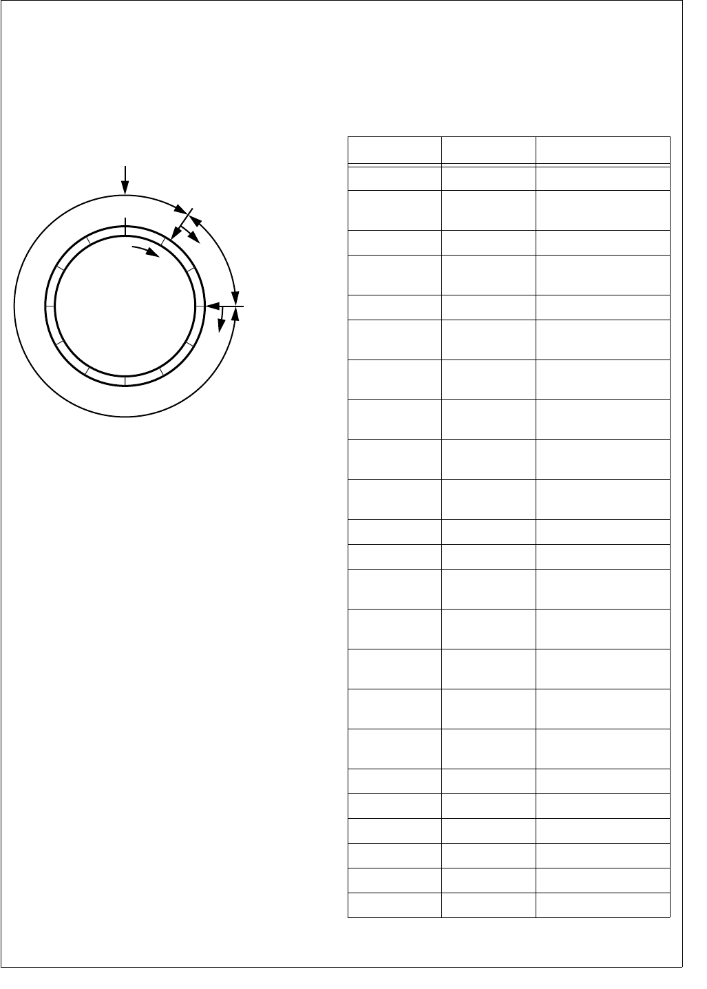
packet is being received on the bus. Figure 32 shows the
detailed behavior of receive FIFOs.
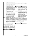
Figure 32. Receive FIFO Operation
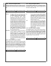
RFnS The Receive FIFO n Size is the total number
of bytes available within the FIFO.
RXRP The Receive Read Pointer is incremented
with every read by software from the receive
FIFO. This pointer wraps around to zero if
RFnS is reached. RXRP is never incremented
beyond the value of RXWP. If an attempt is
made to read more bytes than are actually
available (FIFO underrun), the last byte is
read repeatedly.
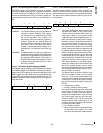
RXWP The Receive Write Pointer is incremented ev-
ery time the Endpoint Controller writes to the
receive FIFO. This pointer wraps around to
zero if RFnS is reached. An overrun condition
occurs if RXRP equals RXWP and an attempt
is made to write an additional byte.
RXFL The Receive FIFO Level indicates how many
more bytes can be received until an overrun
condition occurs with the next write to the
FIFO. A FIFO warning is issued if RXFL de-
creases to a specific value. The respective
WARNn bit in the FWR register is set if RXFL
is equal to or less than the number specified
by the RFWL bit in the RXCn register.
RCOUNT The Receive FIFO Count indicates how many
bytes can be read from the receive FIFO. This
value is accessible by software via the RXSn
register.
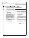
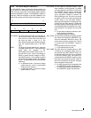
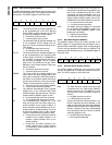
18.3 USB CONTROLLER REGISTERS
The CR16 USB node has a set of memory-mapped regis-
ters that can be read/written from the CPU bus to control the
USB interface. Some register bits are reserved; reading
from these bits returns undefined data. Reserved register
bits must always be written with 0.
FLUSH (Resets RXRP and RXWP)
RXRP
RCOUNT = RXWP
- RXRF
RXWP
RXFL = RXRP
- RXWP (= RFnS - RCOUNT)
RX FIFO n
0X0RFnS
- 1
+
+
+
DS052
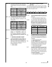
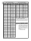
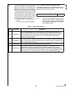
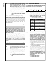
Table 40 USB Controller Registers
Name Address Description
MCNTRL FF FD80h Main Control Register
NFSR FF FD8Ah
Node Functional State
Register
MAEV FF FD8Ch Main Event Register
ALTEV FF FD90h
Alternate Event
Register
MAMSK FF FD8Eh Main Mask Register
ALTMSK FF FD92h
Alternate Mask
Register
TXEV FF FD94h
Transmit Event
Register
TXMSK FF FD96h
Transmit Mask
Register
RXEV FF FD98h
Receive Event
Register
RXMSK FF FD9Ah
Receive Mask
Register
NAKEV FF FD9Ch NAK Event Register
NAKMSK FF FD9Eh NAK Mask Register
FWEV FF FDA0h
FIFO Warning Event
Register
FWMSK FF FDA2h
FIFO Warning Mask
Register
FNH FF FDA4h
Frame Number High
Byte Register
FNL FF FDA6h
Frame Number Low
Byte Register
FAR FF FD88h
Function Address
Register
DMACNTRL FF FDA8h DMA Control Register
DMAEV FF FDAAh DMA Event Register
DMAMSK FF FDACh DMA Mask Register
MIR FF FDAEh Mirror Register
DMACNT FF FDB0h DMA Count Register
DMAERR FF FDB2h DMA Error Register


