29 www.national.com
CP3BT26
7.0 System Configuration Registers
The system configuration registers control and provide sta-
tus for certain aspects of device setup and operation, such
as indicating the states sampled from the ENV[2:0] inputs.
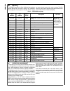
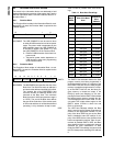
The system configuration registers are listed in Table 9.
7.1 MODULE CONFIGURATION REGISTER
(MCFG)
The MCFG register is a byte-wide, read/write register that
selects the clock output features of the device.
At reset, the register bits are cleared except for the
USB_ENABLE bit, which is set. Initialization software must
write a specific value to this register to enable the SCLK,
MCLK, output pin function.
The register must be written in active mode only, not in pow-
er save, HALT, or IDLE mode. However, the register con-
tents are preserved during all power modes.
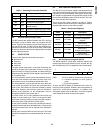
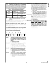
The MCFG register format is shown below.
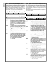
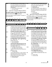
EXIOE The EXIOE bit controls whether the external
bus is enabled in the IRE environment for im-
plementing the I/O Zone (FF FB00h
–FF
FBFFh).
0
– External bus disabled.
1 – External bus enabled.
PLLCLKOE
The PLLCLKOE bit controls whether the PLL
clock is driven on the ENV0/PLLCLK pin.
0
– ENV0/PLLCLK pin is high impedance.
1
– PLL clock driven on the ENV0/PLLCLK
pin.
MCLKOE The MCLKOE bit controls whether the Main
Clock is driven on the ENV1/CPUCLK pin.
0
– ENV1/CPUCLK pin is high impedance.
1
– Main Clock is driven on the ENV1/CPU-
CLK pin.
SCLKOE The SCLKOE bit controls whether the Slow
Clock is driven on the ENV2/SLOWCLK pin.
0
– ENV2/SLOWCLK pin is high impedance.
1
– Slow Clock is driven on the ENV2/SLOW-
CLK pin.
USB_ENABLE
The USB_ENABLE bit can be used to force
an external USB transceiver into its low-power
mode. The power mode is dependent on the
USB controller status, the USB_ENABLE bit
in the Function Word (see Section 8.4.1), and
the USB_ENABLE bit in the MCFG register.
0
– External USB transceiver forced into low-
power mode.
1 – Transceiver power mode dependent on
USB controller status and programming
of the Function Word. (This is the state of
the USB_ENABLE bit after reset.)
MISC_IO_SPEED
The MISC_IO_SPEED bit controls the slew
rate of the output drivers for the ENV[2:0],
RDY
, RFDATA, and TDO pins. To minimize
noise, the slow slew rate is recommended.
0 – Fast slew rate.
1
– Slow slew rate.
MEM_IO_SPEED
The MEM_IO_SPEED bit controls the slew
rate of the output drivers for the A[22:0], RD,
SEL[2:0]
, SELIO, WR[1:0], PB[7:0], and
PC[7:0] pins. Memory speeds for the
CP3BT26 are characterized with fast slew
rate. Slow slew rate reduces the available
memory access time by 5 ns.
0
– Fast slew rate.
1
– Slow slew rate.
Table 9 System Configuration Registers
Name Address Description
MCFG FF F910h
Module Configuration
Register
MSTAT FF F914h
Module Status
Register
7 6 5 4 3 2 1 0
Res.
MEM_IO
_SPEED
MISC_IO
_SPEED
USB
_ENABLE
SCLK
OE
MCLK
OE
PLLCLK
OE
EXI
OE


