www.national.com 38
CP3BT26
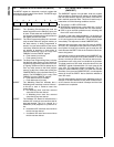
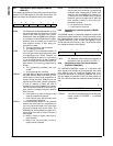
8.5.7 Flash Memory Status Register (FMSTAT/
FSMSTAT)
This register reports the currents status of the on-chip Flash
memory. The FLSR register is clear after device reset. The
CPU bus master has read/write access to this register.
EERR The Erase Error bit indicates whether an error
has occurred during a page erase or module
(block) erase. After an erase error occurs,
software can clear the EERR bit by writing a 1
to it. Writing a 0 to the EERR bit has no effect.
Software must not change this bit while the
flash program memory is busy being pro-
grammed or erased.
0
– The erase operation was successful.
1 – An erase error occurred.
PERR The Program Error bit indicates whether an
error has occurred during programming. After
a programming error occurs, software can
clear the PERR bit by writing a 1 to it. Writing
a 0 to the PERR bit has no effect. Software
must not change this bit while the flash pro-
gram memory is busy being programmed or
erased.
0
– The programming operation was suc-
cessful.
1
– A programming error occurred.
FMBUSY The Flash Memory Busy bit indicates whether
the flash memory (either main block or infor-
mation block) is busy being programmed or
erased. During that time, software must not
request any further flash memory operations.
If such an attempt is made, the CPU is
stopped as long as the FMBUSY bit is active.
The CPU must not attempt to read from pro-
gram memory (including instruction fetches)
while it is busy.
0
– Flash memory is ready to receive a new
erase or programming request.
1
– Flash memory busy with previous erase
or programming operation.
FMFULL The Flash Memory Buffer Full bit indicates
whether the write buffer for programming is
full or not. When the buffer is full, new erase
and write requests may not be made. The
IENPROG bit can be enabled to trigger an in-
terrupt when the buffer is ready to receive a
new request.
0
– Buffer is ready to receive new erase or
write requests.
1
– Buffer is full. No new erase or write re-
quests can be accepted.
DERR The Data Loss Error bit indicates that a buffer
overrun has occurred during a programming
sequence. After a data loss error occurs, soft-
ware can clear the DERR bit by writing a 1 to
it. Writing a 0 to the DERR bit has no effect.
Software must not change this bit while the
flash program memory is busy being pro-
grammed or erased.
0
– No data loss error occurred.
1
– Data loss error occurred.
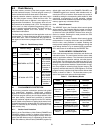
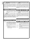
8.5.8 Flash Memory Prescaler Register (FMPSR/
FSMPSR)
The FMPSR register is a byte-wide read/write register that
selects the prescaler divider ratio. The CPU must not modify
this register while an erase or programming operation is in
progress (FMBUSY is set). At reset, this register is initial-
ized to 04h if the flash memory is idle. The CPU bus master
has read/write access to this register.
FTDIV The prescaler divisor scales the frequency of
the System Clock by a factor of (FTDIV + 1).
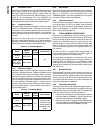
8.5.9 Flash Memory Start Time Reload Register
(FMSTART/FSMSTART)
The FMSTART/FSMSTART register is a byte-wide read/
write register that controls the program/erase start delay
time. Software must not modify this register while a pro-
gram/erase operation is in progress (FMBUSY set). At re-
set, this register is initialized to 18h if the flash memory is
idle. The CPU bus master has read/write access to this reg-
ister.
FTSTART The Flash Timing Start Delay Count field gen-
erates a delay of (FTSTART + 1) prescaler
output clocks.
7 5 4 3 2 1 0
Reserved DERR FMFULL FMBUSY PERR EERR
754 0
Reserved FTDIV
70
FTSTART


