www.national.com 94
CP3BT26
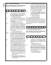
18.3.1 Main Control Register (MCNTRL)
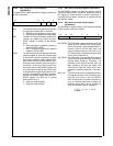
The MCNTRL register controls the main functions of the
CR16 USB node. The MCNTRL register provides read/write
access from the CPU bus. Reserved bits must be written
with 0, and they return 0 when read. It is clear after reset.
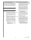
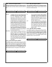
USBEN The USB Enable controls whether the USB
module is enabled. If the USB module is dis-
abled, the 48 MHz clock within the USB node
is stopped, all USB registers are initialized to
their reset state, and the USB transceiver forc-
es SE0 on the bus to prevent the hub from de-
tected the USB node. The USBEN bit is clear
after reset.
0 – The USB module is disabled.
1 – The USB module is enabled.
EPC0 FF FDC0h
Endpoint Control 0
Register
EPC1 FF FDD0h
Endpoint Control 1
Register
EPC2 FF FDD8h
Endpoint Control 2
Register
EPC3 FF FDE0h
Endpoint Control 3
Register
EPC4 FF FDDE8h
Endpoint Control 4
Register
EPC5 FF FDF0h
Endpoint Control 5
Register
EPC6 FF FDF8h
Endpoint Control 6
Register
TXS0 FF FDC4h
Transmit Status 0
Register
TXS1 FF FDD4h
Transmit Status 1
Register
TXS2 FF FDE4h
Transmit Status 2
Register
TXS3 FF FDF4h
Transmit Status 3
Register
TXC0 FF FDC6h
Transmit Command 0
Register
TXC1 FF FDD6
Transmit Command 1
Register
TXC2 FF FDE6h
Transmit Command 2
Register
TXC3 FF FDF6h
Transmit Command 3
Register
TXD0 FF FDC2h
Transmit Data 0
Register
TXD1 FF FDD2h
Transmit Data 1
Register
TXD2 FF FDE2h
Transmit Data 2
Register
TXD3 FF FDF2h
Transmit Data 3
Register
RXS0 FF FDCCh
Receive Status 0
Register
RXS1 FF FDDCh
Receive Status 1
Register
RXS2 FF FDECh
Receive Status 2
Register
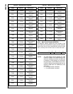
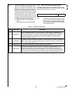
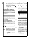
Table 40 USB Controller Registers
Name Address Description
RXS3 FF FDFCh
Receive Status 3
Register
RXC0 FF FDCEh
Receive Command 0
Register
RXC1 FF FDDEh
Receive Command 1
Register
RXC2 FF FDEEh
Receive Command 2
Register
RXC3 FF FDFEh
Receive Command 3
Register
RXD0 FF FDCAh
Receive Data 0
Register
RXD1 FF FDDAh
Receive Data 2
Register
RXD2 FF FDEAh
Receive Data 2
Register
RXD3 FF FDFAh
Receive Data 3
Register
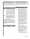
7 4 3 2 1 0
Reserved NAT Reserved USBEN
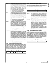
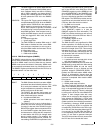
Table 40 USB Controller Registers
Name Address Description


